
PCIe
Overview
Product Versions
| Chip Name | Kernel Version |
|---|---|
| RK1808 | 4.4, 4.19 |
| RK3528 | 4.19, 5.10, 6.1 |
| RK3562 | 5.10, 6.1 |
| RK3566/RK3568 | 4.19, 5.10, 6.1 |
| RK3576 | 6.1 |
| RK3588 | 5.4, 5.10, 6.1 |
Note: RK3399 uses a different PCIe controller IP and is not covered in this document. Please refer to "Rockchip_RK3399_Developer_Guide_PCIe_CN".
Target Audience
This document (guide) is mainly intended for the following engineers:
- Technical Support Engineers
- Software Development Engineers
1. Chip Resource Introduction
1.1 RK1808
| Resource | Mode | Supported Lanes | DMA Support | MMU Support | ASPM Support | Remarks |
|---|---|---|---|---|---|---|
| PCIe Gen2 | RC | x2 lane | No | No | L0s/L1 | Internal clock |
1.2 RK3528
| Resource | Mode | Lane Split Support | DMA Support | MMU Support | ASPM Support | Remarks |
|---|---|---|---|---|---|---|
| PCIe Gen2 x1 | RC | No | No | No | ALL | Internal clock |
1.3 RK3562
| Resource | Mode | Lane Split Support | DMA Support | MMU Support | ASPM Support | Remarks |
|---|---|---|---|---|---|---|
| PCIe Gen2 x1 | RC | No | No | No | ALL | Internal clock |
1.4 RK3566
| Resource | Mode | Lane Split Support | DMA Support | MMU Support | ASPM Support | Remarks |
|---|---|---|---|---|---|---|
| PCIe Gen2 x1 | RC | No | No | No | L0s/L1 | Internal clock |
1.5 RK3568
1.5.1 Controller
| Resource | Mode | Lane Split | DMA Support | MMU Support | ASPM Support | Remarks |
|---|---|---|---|---|---|---|
| PCIe Gen2 | RC | 1 lane only | No | No | L0s/L1 | Internal clock |
| PCIe Gen3 | RC/EP | 1 lane RC + 1 lane RC | 2 read Channels + 2 write Channels | No | ALL | Supports pcie30phy |
| PCIe Gen3 | RC | 1 lane | No | No | ALL | Supports pcie30phy |
1.5.2 PHY
| Resource | dts Node | Reference Clock | Split | Combo |
|---|---|---|---|---|
| pcie30phy | phy@fe8c0000 | External | 2Lane: Default | PCIe dedicated |
| combphy2_psq | phy@fe840000 | Internal/External | 1Lane + 1Lane: rockchip,bifurcation | combo |
Note: pcie30phy 2Lane is by default configured as PCIe Gen3 x 2 lane. After splitting, the "PCIe Gen3 x 2 lane" and "PCIe Gen3 x 1 lane" controllers each use 1 lane.
1.6 RK3576
| Resource | Mode | Lane Split Support | DMA Support | MMU Support | ASPM Support | Remarks |
|---|---|---|---|---|---|---|
| PCIe Gen2 x1 | RC | No | No | Yes | ALL | Internal clock |
1.7 RK3588
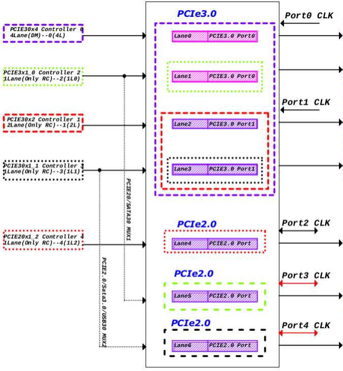
Note: RK3588 has a total of 5 PCIe controllers, with identical hardware IP but different configurations. One 4Lane DM mode can support EP usage, while the other 2Lane and three 1Lane controllers can only be used as RC. RK3588 has two types of PCIe PHY: one is pcie3.0PHY with 2 Ports and 4 Lanes; the other is pcie2.0 PHY, each being 2.0 1Lane, used in combo with SATA and USB. The 4Lane of pcie3.0 PHY can be split as needed. After splitting, the corresponding controllers must be properly configured. All configurations are done in DTS, no driver modification required.
Usage restrictions:
- After splitting pcie30phy, the pcie30x4 controller, when working in 2Lane mode, can only be paired with port0 of pcie30phy; in 1Lane mode, it can only be paired with port0lane0 of pcie30phy;
- After splitting pcie30phy, the pcie30x2 controller, when working in 2Lane mode, can only be paired with port1 of pcie30phy; in 1Lane mode, it can only be paired with port1lane0 of pcie30phy;
- When pcie30phy is split into four 1Lanes, port0lane1 of pcie3phy can only be paired with the pcie2x1l0 controller, and port1lane1 of pcie3phy can only be paired with the pcie2x1l1 controller;
- The pcie30x4 controller working in EP mode can use 4Lane mode, or use 2Lane mode with port0 of pcie30phy. The 2Lane of port1 of pcie30phy can be used as RC with other controllers. By default, when using common clock as the reference clock, it is not possible to have lane0 of port0 of pcie30phy working in EP mode and lane1 working in RC mode with other controllers, because the two lanes of port0 share one input reference clock, and simultaneous use of clock by RC and EP may cause conflicts.
- If only one port of RK3588 pcie30phy is used, the other port also needs to be powered, and other signals such as refclk can be grounded.
1.7.1 Controller
| Resource | Mode | dts Node | Available PHY | Internal DMA | ASPM Support | MMU Support |
|---|---|---|---|---|---|---|
| PCIe Gen3 x4 | RC/EP | pcie3x4: pcie@fe150000 | pcie30phy | 2 read Channels + 2 write Channels | ALL | Yes |
| PCIe Gen3 x2 | RC | pcie3x2: pcie@fe160000 | pcie30phy | No | ALL | Yes |
| PCIe Gen3 x1 | RC | pcie2x1l0: pcie@fe170000 | pcie30phy, combphy1_ps | No | ALL | Yes |
| PCIe Gen3 x1 | RC | pcie2x1l1: pcie@fe180000 | pcie30phy, combphy2_psu | No | ALL | Yes |
| PCIe Gen3 x1 | RC | pcie2x1l2: pcie@fe190000 | combphy0_ps | No | ALL | Yes |
1.7.2 PHY
| Resource | dts Node | Reference Clock | Split | Combo |
|---|---|---|---|---|
| pcie30phy | phy@fee80000 | External | 4Lane: PHY_MODE_PCIE_AGGREGATION 2Lane+2Lane: PHY_MODE_PCIE_NANBNB 2Lane+1Lane+1Lane: PHY_MODE_PCIE_NANBBI 1Lane4: PHY_MODE_PCIE_NABIBI | PCIe dedicated |
| combphy0_ps | phy@fee00000 | Internal/External | - | Combo with SATA |
| combphy1_ps | phy@fee10000 | Internal/External | - | Combo with SATA |
| combphy2_psu | phy@fee20000 | Internal/External | - | Combo with SATA/USB3 |
1.8 RK3588S
Note: The PCIe of RK3588S is relatively simple, with two 1Lane controllers and two 1Lane comboPHYs for PCIe 2.0, in a one-to-one correspondence.
1.8.1 Controller
| Resource | Mode | dts Node | Available PHY | Internal DMA | ASPM Support | MMU Support |
|---|---|---|---|---|---|---|
| PCIe Gen3 x1 | RC | pcie2x1l1: pcie@fe180000 | combphy2_psu | No | ALL | Yes |
| PCIe Gen3 x1 | RC | pcie2x1l2: pcie@fe190000 | combphy0_ps | No | ALL | Yes |
1.8.2 PHY
| Resource | dts Node | Reference Clock | Split | Combo |
|---|---|---|---|---|
| combphy0_ps | phy@fee00000 | Internal/External | - | Combo with SATA |
| combphy2_psu | phy@fee20000 | Internal/External | - | Combo with SATA/USB3 |
2. DTS Configuration
2.1 Key Points for Configuration��
Most PCIe configurations are fixed, and there are not many variables that need to be configured in the board-level dts. Refer to the following key points for configuration:
- Controller/PHY Enable: Enable the correct controller and PHY according to the schematic. Note that the index of the controller and the index of the phy may not match sequentially.
- Controller: Some controllers (such as RK3588's pcie2x1l0 and pcie2x1l1) have multiple PHYs to choose from. Configure "phys" correctly according to the design.
- Controller: As RC, usually need to configure "reset-gpios", corresponding to the "PERSTn" signal of PCIe in the schematic.
- Controller: As RC, may need to configure "vpcie3v3-supply", corresponding to the fixed regulator controlled by the "PWREN" gpio signal of PCIe.
- Controller: When used as EP, need to modify "compatible" to the corresponding string for EP mode.
- PHY: pcie30phy has 4 lanes and can be split. Configure the "rockchip,pcie30-phymode" mode correctly according to the design.
2.2 RK1808 DTS Configuration
For RK1808 dts configuration, all implementation modes have examples in the SDK evb code. You can select the matching content from the table below and copy it to the product board-level dts for use.
| Resource | Mode | Reference Configuration | Controller Node | PHY Node | Remarks |
|---|---|---|---|---|---|
| PCIe Gen2 x2 lane | RC | rk1808-evb.dtsi | pcie0 | combphy | Need to disable usbdrd_dwc3 and usbdrd3 |
| PCIe Gen2 x2 lane | EP | Add compatible = "rockchip,rk1808-pcie-ep","snps,dw-pcie"; to the pcie0 node in rk1808-evb.dtsi | pcie0 | combphy | Need to disable usbdrd_dwc3 and usbdrd3 |
2.3 RK3528 DTS Configuration
For RK3528 dts configuration, all implementation modes have examples in the SDK evb code. You can select the matching content from the table below and copy it to the product board-level dts for use.
| Resource | Mode | Reference Configuration | Controller Node | PHY Node |
|---|---|---|---|---|
| PCIe Gen2 x1 lane | RC | rk3528-evb2-ddr3-v10.dtsi | pcie2x1 | combphy_pu |
2.4 RK356X DTS Configuration
For RK356x dts configuration, all implementation modes have examples in the SDK evb code. You can select the matching content from the table below and copy it to the product board-level dts for use.
2.4.1 RK3562 dts
| Resource | Mode | Reference Configuration | Controller Node | PHY Node |
|---|---|---|---|---|
| PCIe Gen2 x1 lane | RC | rk3562-evb1-lp4x-v10.dtsi | pcie2x1 | combphy_pu |
2.4.2 RK3566 dts
| Resource | Mode | Reference Configuration | Controller Node | PHY Node |
|---|---|---|---|---|
| PCIe Gen2 x1 lane | RC | rk3566-evb1-ddr4-v10.dtsi | pcie2x1 | combphy2_psq |
2.4.3 RK3568 dts
| Resource | Mode | Reference Configuration | Controller Node | PHY Node |
|---|---|---|---|---|
| PCIe Gen2 x1 lane | RC | rk3568-evb2-lp4x-v10.dtsi | pcie2x1 | combphy2_psq |
| PCIe Gen3 x2 lane | RC | rk3568-evb1-ddr4-v10.dtsi | pcie3x2 | pcie30phy |
| PCIe Gen3 split 1 lane | RC | rk3568-evb6-ddr3-v10.dtsi | pcie3x2 | pcie30phy pcie3x1 |
| PCIe Gen3 x2 lane | EP | rk3568-iotest-ddr3-v10.dts | pcie3x2 | pcie30phy |
2.4.4 RK3576 dts
| Resource | Mode | Reference Configuration | Controller Node | PHY Node |
|---|---|---|---|---|
| PCIe Gen2 x1 lane | RC | rk3576-test1.dtsi | pcie0 | combphy0_ps |
| PCIe Gen2 x1 lane | RC | rk3576-test1.dtsi | pcie1 | combphy1_psu |
2.5 RK3588 DTS Configuration
RK3588 has many controllers and PHYs, so it is not possible to enumerate all combinations in the SDK evb code. Just configure according to the key points. Here are some typical examples for reference.
2.5.1 Example 1: pcie3.0 4Lane RC + 2 pcie 2.0 (comboPHY) (RK3588 evb1)
/ {
 vcc3v3_pcie30: vcc3v3-pcie30 {
 compatible = "regulator-fixed";
 regulator-name = "vcc3v3_pcie30";
 regulator-min-microvolt = <3300000>;
 regulator-max-microvolt = <3300000>;
 enable-active-high;
 gpios = <&gpio3 RK_PC3 GPIO_ACTIVE_HIGH>;
 startup-delay-us = <5000>;
 vin-supply = <&vcc12v_dcin>;
 };
};
&combphy1_ps {
 status = "okay";
};
&combphy2_psu {
 status = "okay";
};
&pcie2x1l0 {
 phys = <&combphy1_ps PHY_TYPE_PCIE>;
 reset-gpios = <&gpio4 RK_PA5 GPIO_ACTIVE_HIGH>;
 status = "okay";
};
&pcie2x1l1 {
 phys = <&combphy2_psu PHY_TYPE_PCIE>;
 reset-gpios = <&gpio4 RK_PA2 GPIO_ACTIVE_HIGH>;
 pinctrl-names = "default";
 pinctrl-0 = <&rtl8111_isolate>;
 status = "okay";
};
&pcie30phy {
 rockchip,pcie30-phymode = <PHY_MODE_PCIE_AGGREGATION>;
 status = "okay";
};
&pcie3x4 {
 reset-gpios = <&gpio4 RK_PB6 GPIO_ACTIVE_HIGH>;
 vpcie3v3-supply = <&vcc3v3_pcie30>;
 status = "okay";
};
2.5.2 Example 2: pcie3.0phy split into two 2Lane RC, three PCIe 2.0 1Lane (comboPHY)
/ {
 vcc3v3_pcie30: vcc3v3-pcie30 {
 compatible = "regulator-fixed";
 regulator-name = "vcc3v3_pcie30";
 regulator-min-microvolt = <3300000>;
 regulator-max-microvolt = <3300000>;
 enable-active-high;
 gpios = <&gpio3 RK_PC3 GPIO_ACTIVE_HIGH>;
 startup-delay-us = <5000>;
 vin-supply = <&vcc12v_dcin>;
 };
};
&combphy0_ps {
 status = "okay";
};
&combphy1_ps {
 status = "okay";
};
&combphy2_psu {
 status = "okay";
};
&pcie2x1l0 {
 phys = <&combphy1_ps PHY_TYPE_PCIE>;
 reset-gpios = <&gpio4 RK_PA5 GPIO_ACTIVE_HIGH>;
 vpcie3v3-supply = <&vcc3v3_pcie30>;
 status = "okay";
};
&pcie2x1l1 {
 phys = <&combphy2_psu PHY_TYPE_PCIE>;
 reset-gpios = <&gpio4 RK_PA2 GPIO_ACTIVE_HIGH>;
 vpcie3v3-supply = <&vcc3v3_pcie30>;
 status = "okay";
};
&pcie2x1l2 {
 reset-gpios = <&gpio4 RK_PC1 GPIO_ACTIVE_HIGH>;
 vpcie3v3-supply = <&vcc3v3_pcie30>;
 status = "okay";
};
&pcie30phy {
 rockchip,pcie30-phymode = <PHY_MODE_PCIE_NANBNB>;
 status = "okay";
};
&pcie3x2 {
 reset-gpios = <&gpio4 RK_PB0 GPIO_ACTIVE_HIGH>;
 vpcie3v3-supply = <&vcc3v3_pcie30>;
 status = "okay";
};
&pcie3x4 {
 num-lanes = <2>;
 reset-gpios = <&gpio4 RK_PB6 GPIO_ACTIVE_HIGH>;
 vpcie3v3-supply = <&vcc3v3_pcie30>;
 status = "okay";
};
2.5.3 Example 3: pcie3.0phy split into four 1Lane, one uses PCIe 2.0 1 Lane (comboPHY)
Note
pcie2x1l0/pcie2x1l1are connected to the correspondingTX/RXsignals ofpcie3.0phyin hardware, so disable thecombphy1_ps/combphy2_psunodes in dts.
Reference code
/ {
 vcc3v3_pcie30: vcc3v3-pcie30 {
 compatible = "regulator-fixed";
 regulator-name = "vcc3v3_pcie30";
 regulator-min-microvolt = <3300000>;
 regulator-max-microvolt = <3300000>;
 enable-active-high;
 gpios = <&gpio3 RK_PC3 GPIO_ACTIVE_HIGH>;
 startup-delay-us = <5000>;
 vin-supply = <&vcc12v_dcin>;
 };
};
&combphy0_ps {
 status = "okay";
};
&pcie2x1l0 {
 phys = <&pcie30phy>;
 reset-gpios = <&gpio4 RK_PA5 GPIO_ACTIVE_HIGH>;
 vpcie3v3-supply = <&vcc3v3_pcie30>;
 status = "okay";
};
&pcie2x1l1 {
 phys = <&pcie30phy>;
 reset-gpios = <&gpio4 RK_PA2 GPIO_ACTIVE_HIGH>;
 vpcie3v3-supply = <&vcc3v3_pcie30>;
 status = "okay";
};
&pcie2x1l2 {
 reset-gpios = <&gpio4 RK_PC1 GPIO_ACTIVE_HIGH>;
 vpcie3v3-supply = <&vcc3v3_pcie30>;
 status = "okay";
};
&pcie30phy {
 rockchip,pcie30-phymode = <PHY_MODE_PCIE_NABIBI>;
 status = "okay";
};
&pcie3x2 {
 num-lanes = <1>;
 reset-gpios = <&gpio4 RK_PB0 GPIO_ACTIVE_HIGH>;
 vpcie3v3-supply = <&vcc3v3_pcie30>;
 status = "okay";
};
&pcie3x4 {
 num-lanes = <1>;
 reset-gpios = <&gpio4 RK_PB6 GPIO_ACTIVE_HIGH>;
 vpcie3v3-supply = <&vcc3v3_pcie30>;
 status = "okay";
};
2.6 DTS Property Description
2.6.1 Common Controller DTS Configurations
-
compatible
- Optional: Set whether the PCIe interface uses RC mode or EP mode.
- RK3568 as RC:
compatible = "rockchip,rk3568-pcie", "snps,dw-pcie"; - RK3568 as EP:
compatible = "rockchip,rk3568-pcie-ep", "snps,dw-pcie"; - For RK1808, RK3588: replace
rk3568withrk1808andrk3588respectively.
- RK3568 as RC:
- Optional: Set whether the PCIe interface uses RC mode or EP mode.
-
reset-gpios
- Required: Set the
PERST#reset signal for the PCIe interface.- Example:
reset-gpios = <&gpio3 13 GPIO_ACTIVE_HIGH>; - Note: If multiple lane PCIe interfaces are split, each node needs to configure a different
PERST#signal line.
- Example:
- Required: Set the
-
num-lanes
- Optional: Set the number of lanes used by the PCIe device.
- Example:
num-lanes = <4>; - The default configuration is in the chip-level dtsi. It is recommended to configure according to the actual hardware.
- Example:
- Optional: Set the number of lanes used by the PCIe device.
-
max-link-speed
- Optional: Set the PCIe bandwidth version.
- 1 means Gen1, 2 means Gen2, 3 means Gen3.
- Example:
max-link-speed = <2>; - In principle, it does not need to be configured for every board, only for testing or downgrade purposes.
- Optional: Set the PCIe bandwidth version.
-
status
- Required: Enable both the PCIe controller node and the corresponding phy node.
- Example:
status = "okay";
- Example:
- Required: Enable both the PCIe controller node and the corresponding phy node.
-
vpcie3v3-supply
- Optional: Used to configure the 3V3 power supply for PCIe peripherals (in principle, our hardware reference schematic merges the 12V and 3V3 power supplies of the PCIe slot, so after configuring the 3v3 power supply, the 12V power supply is also controlled together). If the 3V3 for PCIe peripherals needs to be controlled on the board, define a corresponding regulator as shown in the example. For regulator configuration, refer to Documentation/devicetree/bindings/regulator/. Also, if it is a PCIe3.0 controller, an external 100M crystal oscillator chip is generally required. The power supply for this crystal oscillator chip is usually shared with the 3V3 for PCIe peripherals in hardware design. Therefore, after configuring this item, in addition to confirming the 3V3 power supply for peripherals, also confirm whether the external crystal oscillator chip outputs the clock normally. Generally, the external crystal oscillator chip requires a stable period to output the clock. Please strictly refer to the minimum value specified in the clock chip manual, and specify the value of startup-delay-us in the power node with a test margin. For hardware designs with slow discharge after power off, specify the value of off-on-delay-us in the power node to ensure sufficient power cycling. For details, refer to the vcc3v3_pcie node in the rk3568-evb1-ddr4-v10.dtsi file.
-
phys
- Optional: Used to configure the phandle reference of the phy used by the controller. Some controllers can be routed to multiple phys (such as RK3588's pcie2x1l0 and pcie2x1l1). Note that different phys may have different reference methods. comboPHY needs to specify the working mode of the phy at the same time, as follows:
- Example:
phys = <&pcie30phy>;
phys = <&combphy1_ps PHY_TYPE_PCIE>;
- Example:
- Optional: Used to configure the phandle reference of the phy used by the controller. Some controllers can be routed to multiple phys (such as RK3588's pcie2x1l0 and pcie2x1l1). Note that different phys may have different reference methods. comboPHY needs to specify the working mode of the phy at the same time, as follows:
-
rockchip,bifurcation
- Optional: This is a special configuration for the RK3568 chip. It can split the two lanes of pcie3x2 into two 1-lane controllers. The specific configuration method is to enable both the pcie3x1 and pcie3x2 controller nodes and the pcie30phy in dts, and add the rockchip,bifurcation property to both the pcie3x2 and pcie3x1 nodes. Refer to rk3568-evb6-ddr3-v10.dtsi. Otherwise, by default, the pcie3x1 controller cannot be used.
At this time, lane0 is used by the pcie3x2 controller, and lane1 is used by the pcie3x1 controller. The hardware layout strictly follows our schematic. Also note that in this mode, both 1-lane controllers must work in RC mode.
Also pay special attention: after PCIe 3.0 is split into two single lanes and connected to two different peripherals, since the crystal oscillator and its power supply are controlled by the same circuit, do not configure vpcie3v3-supply for only one controller. Otherwise, the controller that obtains the 3v3 voltage operation permission will interfere with the normal initialization of the peripheral connected to the other controller. In this case, the regulator corresponding to vpcie3v3-supply should be configured as regulator-boot-on and regulator-always-on.
-
prsnt-gpios = <&gpio4 15 GPIO_ACTIVE_LOW>;
- Optional configuration: Used for the driver to detect the presence of peripherals and related circuits. If a valid level is detected, the device detection process is skipped. According to the PCIe electrical specification, this GPIO being low indicates a device is present. If your board design is the opposite, you can change it to GPIO_ACTIVE_HIGH to indicate high level means device present. This signal allows the same software to support both products with and without PCIe3 on the same board type, avoiding system exceptions such as rcu stall during PCIe controller initialization.
rockchip,perst-inactive-ms = <500>;
- Optional configuration: Used to configure the reset time of the device #PERST reset signal, in milliseconds. According to the PCIe Express Card Electromechanical Spec, the minimum requirement from downstream device power stable to #PERST release is 100ms. If not configured, the RK driver defaults to 200ms. If this still does not meet the peripheral's requirements, you can adjust as needed based on actual testing.
rockchip,s2r-perst-inactive-ms = <1>;
- Optional configuration: Used to configure the reset time of the device #PERST signal during suspend/resume, in milliseconds. If not configured, its value is the same as rockchip,perst-inactive-ms. If the peripheral is not powered off during suspend, such as Wi-Fi, then #PERST remains in reset during suspend, so the reset time during resume can be shortened, even set to 0.
rockchip,wait-for-link-ms = <1>;
- Optional configuration: Used to configure the wait time after releasing the device #PERST reset signal, in milliseconds. This is for peripherals that require a longer internal initialization time, to prevent system link timeout due to slow initialization. Common devices needing this are FPGAs and some AI accelerator cards.
- supports-clkreq
- Optional configuration: Only valid in RC mode. Please ensure the CLKREQ# pinctrl iomux is set to function io. If this property exists, it indicates that there is a CLKREQ# signal route from the root port to the downstream device, and the host bridge driver can program accordingly. For example, if there is no CLKREQ# signal, the root port will be set to not support PM L1 Substates.
- rockchip,lpbk-master
- Special debug configuration: This is for loopback signal testing, using the PCIe controller to simulate a loopback master environment, letting the device under test enter slave mode. Do not configure this unless you are doing simulation lab RX loopback tests. Note that Gen3 controllers may require compliance mode for loopback slave mode. If you do not understand loopback testing, this is not the configuration you are looking for, do not ask about it.
- rockchip,compliance-mode
- Special debug configuration: This is for compliance signal testing, forcing the PCIe controller into compliance test mode or keeping it powered on after entering test mode with an SMA fixture. This is an array with two values: the first is the test mode, the second is the preset value for that mode. If using an SMA fixture, configure
rockchip,compliance-mode=<0 0>;. If testing soldered devices, fix the mode and preset values,rockchip,compliance-mode=<mode preset>;. Mode can be 1, 2, or 3, representing 2.5GT, 5.0GT, and 8GT signals. Only in 5GT and 8GT modes, preset values 0-10 are valid, representing P0-P10 protocol pre-emphasis settings. See the appendix "PCIe TX Pre-emphasis Preset Table" for details.
- rockchip,keep-power-in-suspend
- Optional configuration: Only valid in RC mode. Used to keep the peripheral powered and reset during suspend. Allows the peripheral to work offline after system suspend. This mode also requires the pcie node to reference
vpcie3v3-supply.
2.6.2 comboPHY dts configuration
- The following configurations do not apply to the combphy node of RK1808.
- The number in the
combphynode indicates the Mux relationship, and the suffix indicates the multiplexing relationship:p,s,u,qrepresent PCIe, SATA, USB, QSGMII respectively.
- rockchip,ext-refclk
-
Special debug configuration: Note this is only for combophy. By default, combophy uses the SoC internal clock. For example, in RK356X, see the rk3568.dtsi node, which uses a 24MHz clock source by default. Besides 24MHz, 25M and 100M are also supported, just set
assigned-clock-rates = <24000000>to the desired frequency. The internal clock is the most cost-effective and is the SDK default, but combophy still reserves the option for an external crystal oscillator. If you need to use an external oscillator, add rockchip,ext-refclk to the combphy node used by the PCIe controller in the board dts, and setassigned-clock-rates = <frequency>to specify the external oscillator frequency, still only supporting 24M, 25M, 100M.- rockchip,enable-ssc
- Special debug configuration: Only for the combphy node used by PCIe. By default, combophy output clock does not enable spread spectrum. If you need to mitigate EMI issues, add this property to the corresponding combphy node to enable SSC.
2.6.3 pcie30phy dts configuration
- rockchip,pcie30-phymode
- Optional configuration: This configures the pcie30phy combination mode, which must be set correctly. Default is 4Lane shared. For details, see
include/dt-bindings/phy/phy-snps-pcie3.h:
- Optional configuration: This configures the pcie30phy combination mode, which must be set correctly. Default is 4Lane shared. For details, see
/*
* pcie30_phy_mode[2:0]
* bit2: aggregation
* bit1: bifurcation for port 1
* bit0: bifurcation for port 0
*/
#define PHY_MODE_PCIE_AGGREGATION 4 /* PCIe3x4 */
#define PHY_MODE_PCIE_NANBNB 0 /* P1:PCIe3x2 + P0:PCIe3x2 */
#define PHY_MODE_PCIE_NANBBI 1 /* P1:PCIe3x2 + P0:PCIe3x1*2 */
#define PHY_MODE_PCIE_NABINB 2 /* P1:PCIe3x1*2 + P0:PCIe3x2 */
#define PHY_MODE_PCIE_NABIBI 3 /* P1:PCIe3x1*2 + P0:PCIe3x1*2 */
2.7 Fill in DTS according to schematic
2.7.1 Low-speed IO description
PCIe module chip signal connections, besides data lines and reference clock differential pairs, may also have the following low-speed IOs:
IO Name RC Mode EP Mode Description PERSTn GPIO output Connect nPOR Required, configure dts "reset-gpios"WAKE GPIO (PMU domain) GPIO output Optional, function driver registers GPIO interrupt and wake source, not handled by PCIe controller driver PWREN GPIO output None Optional, configure dts "vpcie3v3-supply"CLKREQ FUNCTION FUNCTION Optional, used for L1SS, configure dts "supports-clkreq"PRSNT GPIO input None Optional, configure dts "prsnt-gpios"- Only
CLKREQuses PCIe function; this signal is only needed for L1SS. Otherwise, it can be left unconnected. If used, the corresponding dts property must be added. - Other signals use GPIO function; do not configure them as PCIe function in pinctrl. See dts configuration instructions for details.
- The
PERSTsignal is required by the protocol; other signals are configured as needed for the project.
2.7.2 DTS configuration method
The schematic describes hardware from the IO signal perspective, and IO signals are strongly related to PHY index, but the controller and PHY index of RK3588 may not match, so pay special attention when reading the schematic.
Recommended steps for filling in dts based on the hardware schematic:
- Confirm PCIe device allocation:
- Confirm with hardware engineers how many PCIe devices are used and how the chip's PCIe interfaces are allocated.
- Find PHY output:
- In the schematic, find which PHY output the PCIe data lines for each device use.
- Determine controller and PHY:
- Determine which controller and PHY each device uses, and enable them in dts.
- Check controller
phyproperty:- Ensure the controller dts
"phy"property and mode are correct, e.g.,pcie2x1lncontroller should usecomboPHYand specifyPHY_TYPE_PCIE.
- Ensure the controller dts
- Disable other controllers:
- If
comboPHYmay be shared bySATA,USB,RGMII, etc., ensure other controllers are disabled in dts.
- If
- Configure PHY mode:
- Ensure the PHY has the correct working mode, e.g., pcie30phy split combinations must be configured correctly.
- Configure
PERSTnsignal:- Ensure the correct GPIO for
PERSTnis configured in the controller dts node.
- Ensure the correct GPIO for
- Configure
PWRENsignal:- Ensure the correct GPIO for
PWRENis configured in the controller dts node (or in the onboard peripheral dts).
- Ensure the correct GPIO for
- Configure other peripheral hardware:
- Configure other hardware required for the peripheral.
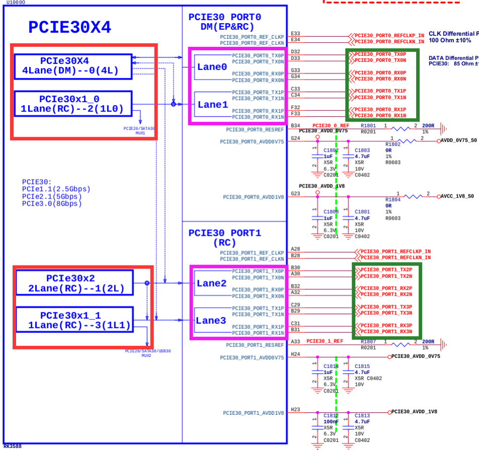
The following diagram shows RK3588 pcie30phy and its possible controllers. Red boxes are controllers, pink boxes are PHY signals, green boxes are peripheral signals. Which controller is used can be confirmed by peripheral signal connections or by checking with hardware engineers. This diagram is from RK3588 evb1, with a PCIe3.0 x4 slot connected, so the controller used is PCIe30X4 (dts name pcie3x4), and other controllers are not used with this PHY.
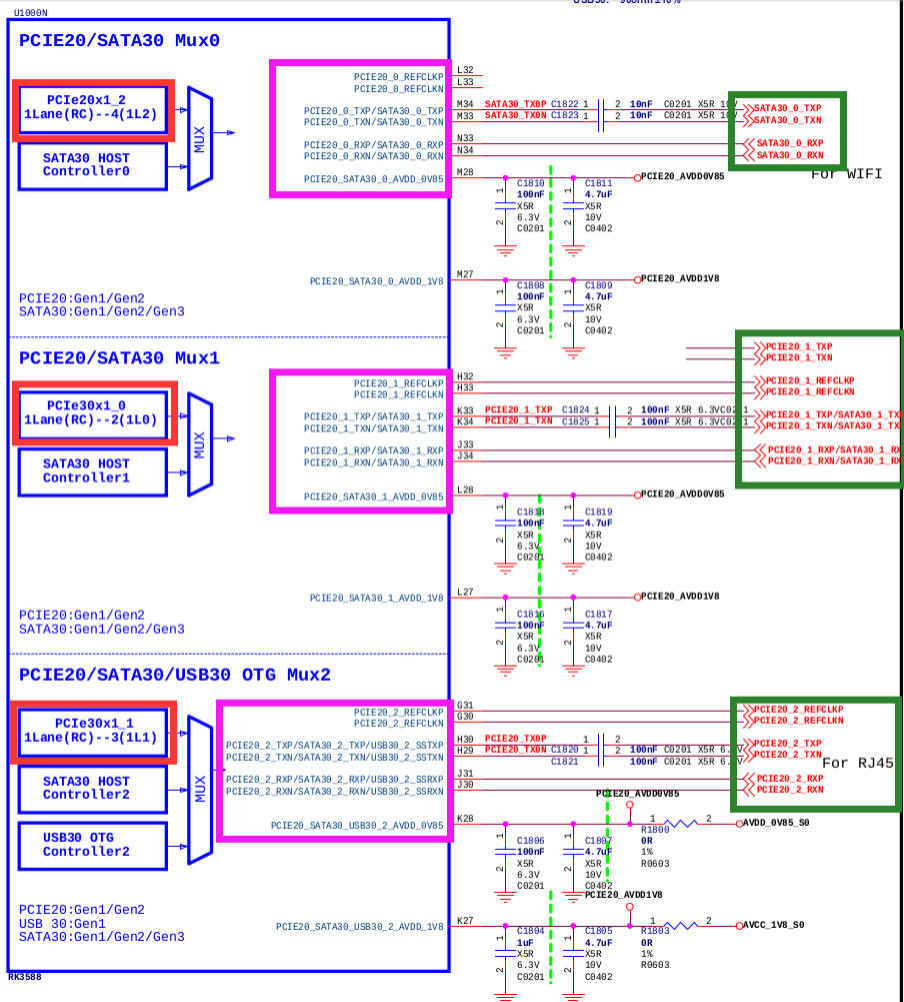
The following diagram shows RK3588 comboPHY and its possible controllers. Red boxes are controllers, pink boxes are PHY signals, green boxes are peripheral signals. Which controller is used can be confirmed by peripheral signal connections or by checking with hardware engineers. In this diagram, Mux0's PHY (combphy0_ps) is in SATA mode, not PCIe; Mux1's PHY (combphy1_ps) works with PCIe30x1_0 (dts name pcie2x1l0) and may be in PCIe mode, depending on the connected device; Mux2's PHY (combphy2_psu) works with PCIe30x1_1 (dts name pcie2x1l1) in PCIe mode to connect a PCIe NIC.
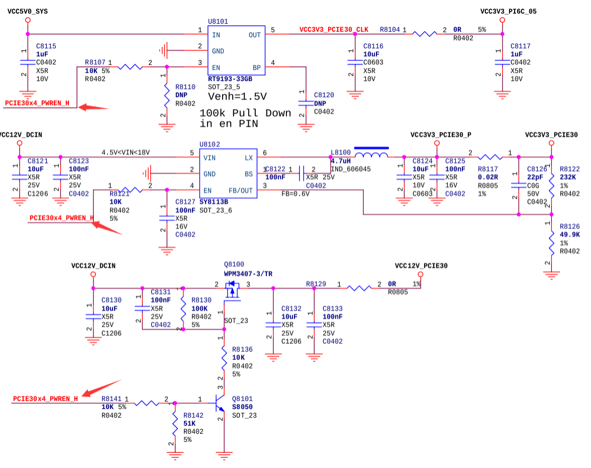
The following diagram shows the PCIe3.0 interface power supply on RK3588 evb1. You can locate the corresponding RK3588 GPIO by the PCIE30X4_PWREN_H signal, then fill it in the pcie3x4 controller dts.
2.8 Wi-Fi module device tree example
Since Wi-Fi modules are usually connected to PCIe2.0 ports, and their use of
combphyis complex, with different power, suspend, and reset requirements from other devices, here is a device tree example for reference.- Check the schematic to determine which combphy the Wi-Fi module uses. The combphy node number indicates the Mux relationship, and the suffix indicates the multiplexing: p, s, u, q represent PCIe, SATA, USB, QSGMII. In this example, Wi-Fi is connected to the PCIe/SATA muxed
PCIE20/SATA30 Mux0, so configure the combphy0_ps node.
- Search the dts file to ensure other controllers sharing this combphy are disabled to prevent signal interference.
- Move the wifi_reg_on signal from the wireless_wlan node to the PCIe 3.3v power control node.
- If Wi-Fi needs L1.x power mode, see the "RC mode PM L1 Substates support" section.
- If Wi-Fi needs wireless wakeup, ensure wifi_reg_on pin stays high during suspend, and wifi_host_wake pin is connected to a non-power-off PMU IO to generate an interrupt to wake the host. For hardware and software details, see the relevant chapters in our SDK documentation "Rockchip_Developer_Guide_Linux_WIFI_BT_CN.pdf".
- rockchip,enable-ssc
-
      + vcc3v3_pcie20_wifi: vcc3v3-pcie20-wifi {
      +     compatible = "regulator-fixed";
      +     regulator-name = "vcc3v3_pcie20_wifi";
      +     regulator-min-microvolt = <3300000>;
      +     regulator-max-microvolt = <3300000>;
      +     enable-active-high;
      +   /*
      +     * wifi_reg_on is enabled after vbat and vddio are stable, and pulled high before reset-gpios,
      +     * so putting it in the PCIe power node meets the module timing, referencing wifi_poweren_gpio.
      +     */
      +     pinctrl-0 = <&wifi_poweren_gpio>;
      +     startup-delay-us = <5000>;
      +     vin-supply = <&vcc12v_dcin>;
      +   };
        wireless_wlan: wireless-wlan {
            compatible = "wlan-platdata";
            wifi_chip_type = "ap6275p";
            pinctrl-names = "default";
            pinctrl-0 = <&wifi_host_wake_irq>;
            WIFI,host_wake_irq = <&gpio0 RK_PA0 GPIO_ACTIVE_HIGH>;
      +       /* Note: wifi_reg_on pin also needs to be configured here for WiFi driver control */
      +       WIFI,poweren_gpio = <&gpio0 RK_PC7 GPIO_ACTIVE_HIGH>;
            status = "okay";
        };
      +
      +&sata0 {
      +   status = "disabled" /* sata0 shares combphy0_ps with pcie2x1l2, must be disabled */
      +}
      +
      +&combphy0_ps {
      +   status = "okay"; /* Ensure phy is enabled */
      +};
      +
      +&pcie2x1l2 {
      +   reset-gpios = <&gpio3 RK_PD1 GPIO_ACTIVE_HIGH>;
      +   rockchip,skip-scan-in-resume;
      +   rockchip,perst-inactive-ms = <500>; /* Refer to Wi-Fi module manual for required #PERST reset time */
      +   vpcie3v3-supply = <&vcc3v3_pcie20_wifi>;
      +   status = "okay";
      +};
      &pinctrl {
          wireless-wlan {
              wifi_poweren_gpio: wifi-poweren-gpio {
      +           //PCIE REG ON: Must be configured as pull-up
      +           rockchip,pins = <0 RK_PC7 RK_FUNC_GPIO &pcfg_pull_up>;
              };
          };
      };
3. menuconfig configuration
- Make sure the following configs are enabled to use PCIe features correctly
CONFIG_PCI=y
CONFIG_PCI_DOMAINS=y
CONFIG_PCI_DOMAINS_GENERIC=y
CONFIG_PCI_SYSCALL=y
CONFIG_PCI_BUS_ADDR_T_64BIT=y
CONFIG_PCI_MSI=y
CONFIG_PCI_MSI_IRQ_DOMAIN=y
CONFIG_PHY_ROCKCHIP_SNPS_PCIE3=y
CONFIG_PHY_ROCKCHIP_NANENG_COMBO_PHY=y
CONFIG_PCIE_DW=y
CONFIG_PCIE_DW_HOST=y
CONFIG_PCIE_DW_ROCKCHIP=y
CONFIG_PCIEPORTBUS=y
CONFIG_PCIE_PME=y
CONFIG_GENERIC_MSI_IRQ=y
CONFIG_GENERIC_MSI_IRQ_DOMAIN=y
CONFIG_IRQ_DOMAIN=y
CONFIG_IRQ_DOMAIN_HIERARCHY=y
- Enable NVMe devices (PCIe SSDs), PCIe-to-AHCI devices (SATA), PCIe-to-USB devices (XHCI) are enabled by default config, please confirm. For other devices such as Ethernet cards, WiFi, please check the relevant config yourself.
CONFIG_BLK_DEV_NVME=y
CONFIG_SATA_PMP=y
CONFIG_SATA_AHCI=y
CONFIG_SATA_AHCI_PLATFORM=y
CONFIG_ATA_SFF=y
CONFIG_ATA=y
CONFIG_USB_XHCI_PCI=y
CONFIG_USB_XHCI_HCD=y
Note: The default kernel only supports PCIe-to-SATA devices listed in drivers/ata/ahci.c. For others, please contact the manufacturer or agent for support.
4. Standard EP function development
Some Rockchip chips' PCIe controllers support EP mode, allowing the chip to be developed as a standard PCIe EP product. For EP function implementation, see the document "Rockchip_Developer_Guide_PCIE_EP_Stardard_Card_CN".
5. RC mode PM L1 Substates Support
When it is confirmed that both the RK host controller and the connected peripherals support PCIe PM L1 Substates, you can enable the PM L1 Substates feature to further optimize power consumption.
It is further emphasized that if there are devices in the target peripherals that do not support PM L1 Substates, especially if the motherboard is designed for slot external non-fixed devices, do not enable the PM L1 Substates feature, otherwise some devices may not work properly.
Hardware Circuit Design Supporting PM L1 Substates
RC CLKREQ#, EP CLKREQ# are interconnected at both ends.
Optional optimization: For the external reference clock scheme, you can consider connecting CLKREQ# to CLOCK_GEN OE. If CLOCK_GEN OE is active high, an inverter should be added.
System Default Settings
System support for PM L1 Substates is disabled:
- The dts does not add the
supports-clkreq;property - Kernel macro configuration
CONFIG_PCIEASPM_POWER_SUPERSAVE=n
Enabling PM L1 Substates Support in the System
- Confirm that both RC/EP support PM L1 Substates. For RC support, refer to the "Chip Resource Introduction" chapter under the ASPM section.
- Hardware configuration of the CLKREQ# signal: Ensure compliance with the "Hardware Circuit Design Supporting PM L1 Substates"
- Software configuration of the CLKREQ# signal: Set the CLKREQ# iomux to function io
- Add the
supports-clkreq;property to the controller node in the software configuration. For details, refer to "dts Configurable Item 11" - Enable PM L1 Substates support:
- Method 1: Kernel macro configuration
CONFIG_PCIEASPM_POWER_SUPERSAVE=y - Method 2: Some peripherals such as WIFI support enabling PM L1 Substates in the driver
- Method 1: Kernel macro configuration
Note:
- If you try to enable the kernel macro configuration without strictly meeting the above conditions, the PCIe link may enter an abnormal state and fail to wake up.
- Please ensure that the kernel source code is up-to-date and includes the L1SS support patch: commit e18dfa93 PCI: rockchip: dw: Support PM L1 clock removing
6. GPIO-based Hotplug Detection Mechanism
6.1 Hardware Requirements
- The PRSNT#_1 of the PCIe slot needs to be connected to any GPIO of the host controller as a detection pin.
- The power supply of the PCIe device needs to be software-controllable for power on/off.
6.2 Software Requirements
- At least include the following commits. If not, please contact the business for patches:
commit 4de1a0c19e0f9804ba22e7f5e544fea317913957
Author: Shawn Lin <shawn.lin@rock-chips.com>
Date:   Tue Mar 12 16:38:46 2024 +0800

PCI: rockchip: dw: Add gpio based hotplug
Change-Id: I49c57755d11cc43bbf7cf9eb23542f5e1e11aaa3

commit 86f3010d7f523c9f5a2e88d9f8f1871ed89da098
Author: Vidya Sagar <vidyas@nvidia.com>
Date:   Sat Oct 1 00:57:45 2022 +0530

FROMLIST: PCI/hotplug: Add GPIO PCIe hotplug driver
Change-Id: Iafa798ee4d98f195f5d33d80120da0c569132548
- The kernel must confirm the following configurations are enabled:
CONFIG_HOTPLUG_PCI=y
CONFIG_HOTPLUG_PCI_GPIO=y
- DTS configuration reference:
&pcie0 {
  reset-gpios = <&gpio4 RK_PC7 GPIO_ACTIVE_HIGH>;
  vpcie3v3-supply = <&vcc3v3_pcie0>;
  hotplug-gpios = <&gpio4 RK_PC4 IRQ_TYPE_EDGE_BOTH>;
  pinctrl-names = "default";
  pinctrl-0 = <&hot_plug0>;
  status = "okay";
};
&pinctrl {
  pcie {
      hot_plug0: hot-plug0 {
          rockchip,pins = <4 RK_PC4 RK_FUNC_GPIO &pcfg_pull_up>;
     };
 };
};
6.3 Usage Restrictions
- Hot-plugging PCIe devices while powered can easily damage the device and the host controller. The device removal and power-off process takes some time after device removal, so rapid hot-plugging is prohibited. You need to wait until the following removal log appears before reinserting:
[   35.680289][  T134] pcieport 0000:00:00.0: Hot-UnPlug Event
[   35.680361][  T134] pcieport 0000:00:00.0: Power Status = 1
[   35.827183][  T134] rk-pcie 2a200000.pcie: rk_pcie_slot_disable
[   35.827303][  T134] pcieport 0000:00:00.0: Hot-UnPlug Event
[   35.827323][  T134] pcieport 0000:00:00.0: Power Status = 0
[   35.827334][  T134] pcieport 0000:00:00.0: Device is already removed
-
To ensure data integrity and system stability, make sure the system stops accessing the device to be removed.
-
It is not possible to support individual hot-plugging of downstream devices under a switch. If this is required, first confirm that the switch supports individual hot-plugging of downstream devices, then refer to the "How to rescan or replace a single downstream device online?" section in common application issues for rescan processing, which can achieve the same effect.
-
Detection of device insertion or removal is not supported in suspend or standby states.
7. Kernel DMATEST
Before development, please confirm whether the target PCIe controller supports DMA transfer. For details, refer to the "Chip Resource Introduction" chapter.
RK PCIe DMA provides a test mechanism based on the kernel module_param mechanism, similar to Linux dmatest. You can further complete PCIe DMA applications under the kernel based on this framework.
Kernel Version Requirements
At least include the following commit. If not, please contact the business for patches:
commit a7c40cb119703e566d9d5befb8c1a7b0533dd7b7
Author: Jon Lin <jon.lin@rock-chips.com>
Date:   Tue Jan 17 17:46:48 2023 +0800
    PCI: rockchip: dw-dmatest: Suppport rc dma
    1.Set rc dma as default
    2.Changet to ep dma by sending command:
            echo 0 > ./sys/module/pcie_dw_dmatest/parameters/is_rc
    Change-Id: I9b16c328c08f220772e487c7c796b8898d74ae10
    Signed-off-by: Jon Lin <jon.lin@rock-chips.com>
Test Macro Configuration
CONFIG_PCIE_DW_DMATEST=y
CONFIG_ROCKCHIP_PCIE_DMA_OBJ=n
Setup Environment
PCIe interconnection model:
- Customers can build their own RK RC - FPGA EP environment
- RK local test setup: RK RC (RK dmatest configuration) - RK EP (RK chip interconnection configuration)
Note:
- MPS is configured as 256B
- Both RC and EP need reserved memory. It is recommended to reserve 64MB of test memory at 0x3c000000 (default test address)
- It is recommended to disable other unrelated PCIe controllers
Test
For details, refer to the pcie-dw-misc-dmatest.c source code
static int size = 0x20;
module_param(size, int, 0644);
MODULE_PARM_DESC(size, "each packet size in bytes");

static unsigned int cycles_count = 1;
module_param(cycles_count, uint, 0644);
MODULE_PARM_DESC(cycles_count, "how many erase cycles to do (default 1)");

static bool irq;
module_param(irq, bool, 0644);
MODULE_PARM_DESC(irq, "Using irq? (default: false)");

static unsigned int chn_en = 1;
module_param(chn_en, uint, 0644);
MODULE_PARM_DESC(chn_en, "Each bits for one dma channel, up to 2 channels, (default enable chanel 0)");

static unsigned int rw_test = 3;
module_param(rw_test, uint, 0644);
MODULE_PARM_DESC(rw_test, "Read/Write test, 1-read 2-write 3-both(default 3)");

static unsigned int bus_addr = 0x3c000000;
module_param(bus_addr, uint, 0644);
MODULE_PARM_DESC(bus_addr, "Dmatest chn0 bus_addr(remote), chn1 add offset 0x100000, (default 0x3c000000)");

static unsigned int local_addr = 0x3c000000;
module_param(local_addr, uint, 0644);
MODULE_PARM_DESC(local_addr, "Dmatest chn0 local_addr(local), chn1 add offset 0x100000, (default 0x3c000000)");

static unsigned int test_dev;
module_param(test_dev, uint, 0644);
MODULE_PARM_DESC(test_dev, "Choose dma_obj device,(default 0)");

static bool is_rc = true;
module_param_named(is_rc, is_rc, bool, 0644);
MODULE_PARM_DESC(is_rc, "Test port is rc(default true)");
Example 1: RC device, channel 0, write data, data size 1MB, 1000 cycles, local address 0x3c000000, remote address 0x3c000000:
echo 0 > ./sys/module/pcie_dw_dmatest/parameters/test_dev
echo 1 > ./sys/module/pcie_dw_dmatest/parameters/is_rc
echo 1 > ./sys/module/pcie_dw_dmatest/parameters/chn_en
echo 1 > ./sys/module/pcie_dw_dmatest/parameters/rw_test
echo 0x100000 > ./sys/module/pcie_dw_dmatest/parameters/size
echo 1000 > ./sys/module/pcie_dw_dmatest/parameters/cycles_count
echo 0x3c000000 > ./sys/module/pcie_dw_dmatest/parameters/local_addr
echo 0x3c000000 > ./sys/module/pcie_dw_dmatest/parameters/bus_addr
echo run > ./sys/module/pcie_dw_dmatest/parameters/dmatest
Example 2: EP device, channel 0/1 (dual threads running simultaneously), read and write data, data size 8KB, 10000 cycles, local address 0x3c000000, remote address 0x3c000000:
echo 0 > ./sys/module/pcie_dw_dmatest/parameters/test_dev
echo 0 > ./sys/module/pcie_dw_dmatest/parameters/is_rc
echo 3 > ./sys/module/pcie_dw_dmatest/parameters/chn_en
echo 3 > ./sys/module/pcie_dw_dmatest/parameters/rw_test
echo 0x2000 > ./sys/module/pcie_dw_dmatest/parameters/size
echo 10000 > ./sys/module/pcie_dw_dmatest/parameters/cycles_count
echo 0x3c000000 > ./sys/module/pcie_dw_dmatest/parameters/local_addr
echo 0x3c000000 > ./sys/module/pcie_dw_dmatest/parameters/bus_addr
echo run > ./sys/module/pcie_dw_dmatest/parameters/dmatest
8. Kernel Stability Statistics Information
If the PCIe device exhibits abnormal behavior during long-term operation and its running state does not meet expectations, you can try to obtain information from the debugfs node for analysis. To enable this feature, make sure the following commit is included (pcie: rockchip: dw: Add debugfs support), otherwise you can obtain 0001-pcie-rockchip-dw-Add-debugfs-support.patch from the Redmine system as shown in the appendix.
Usage
- Identify the controller address node where the problematic device is located. You can check it from the boot enumeration log or directly from the dtsi.
- Take fe16000.pcie as an example, enter the
/sys/kernel/debug/fe160000.pciedirectory. echo disable > err_eventto disable all event statistics functions.echo clear > err_eventto clear all event statistics counters.echo enable > err_eventto enable all event statistics functions.- Start device aging and reproduce your abnormal case. After reproduction, execute
cat dumpfifoandcat err_event. - Compare the exported information with the Debugfs export information analysis table in the appendix of this document to roughly identify the problem.
9. Kernel Error Injection Test Support
If you need to test the RC-side function driver, business model/EP-side firmware/dual-end hardware IP fault tolerance for PCIe link, you can enable error injection testing to simulate possible error types during interaction and evaluate the stability of dual-end software and IP.
Usage
(1) The following commit is required:
commit fe835d5fd3329ba629f8c4290c818ef4b8f9895d
Author: Shawn Lin <shawn.lin@rock-chips.com>
Date:   Wed Sep 4 17:04:37 2024 +0800
   PCI: rockchip: dw: Add fault injection support
   Change-Id: Ib214cc1be565bf16bafb6a847215572f35c43753
(2) The feature described in the "Kernel Stability Statistics Information" section of this document must be enabled, and enter the corresponding controller directory.
(3) echo "einj_number enable_or_disable error_type error_number" >
fault_injection
   |-------------------|--------------------------------------------------------
--|
   | Value             |         Meaning
|
   |-------------------|--------------------------------------------------------
--|
   |einj_number:       |Error injection group number, only supports 0 to 6, other values are invalid
  |
   |-------------------|--------------------------------------------------------
--|
   |enable_or_disable: |Enable or disable error injection, 0 means disable, 1 means enable, other values are invalid
  |
   |-------------------|--------------------------------------------------------
--|
   |error_type:       |Error injection type selection, select the error type corresponding to the group number according to the appendix|
   |-------------------|--------------------------------------------------------
--|
   |error_number:     |Number of error injections, only supports 0 to 255, other values are invalid
  |
   |-------------------|--------------------------------------------------------
--|
   For example, echo "2 1 2 128" > fault_injection means to enable einj2 and inject 128 NAK DLLP packets.
(4) Start PCIe link transmission, for example NVMe: dd if=/dev/nvme0n1 of=/dev/null bs=1M count=5000
(5) Check if the error occurred: cat err_event
   Rx Recovery Request: 0x1f
   ...
   Tx Nak DLLP: 0x80
(6) Analyze the dual-end software and hardware to see if unexpected software or hardware exceptions occur.
10. Kernel PMU perf Support
10.1 Software and Configuration
(1) The following five commits are required:
commit 0270f32f207f5682a729c17e977eb87bba83823e
Author: Shuai Xue <xueshuai@linux.alibaba.com>
Date:   Fri Dec 8 10:56:50 2023 +0800
   UPSTREAM: PCI: Move pci_clear_and_set_dword() helper to PCI header
   Change-Id: I35125190a4dd8ba25e6ec14b4712750605c22285
commit 1b627c690ade9a72e3cd488e2e11edffb5d0e879
Author: Shuai Xue <xueshuai@linux.alibaba.com>
Date:   Fri Dec 8 10:56:49 2023 +0800
   UPSTREAM: PCI: Add Alibaba Vendor ID to linux/pci_ids.h
   Change-Id: I86188f119a42548ab777df0449f7d0a933f34d12
commit dcfa6c8947baeac74ab44ea8f03d3831a062c14b
Author: Shuai Xue <xueshuai@linux.alibaba.com>
Date:   Fri Dec 8 10:56:51 2023 +0800
   BACKPORT: drivers/perf: add DesignWare PCIe PMU driver
   Change-Id: I470f4dc2791168760517c77dd31a4dacd7dab591
commit 6cb6a00862fa29f815412634569e2015f86e397a
Author: Shawn Lin <shawn.lin@rock-chips.com>
Date:   Tue Sep 3 16:24:36 2024 +0800
   perf/dwc_pcie: Add support for Rockchip vendor devices
   Change-Id: I6fde80440d2fa058b38a7d927eb846f477812b5f
commit 50cb3fcd18fb9defe23ba95eb3962a287e957166
Author: Shawn Lin <shawn.lin@rock-chips.com>
Date:   Tue Sep 3 16:24:36 2024 +0800
   PCI: rockchip: dw: Add dwc pmu support for rockchip
   Change-Id: Ia27ee055aa3e63deeb7fd646411c3542b7019288
(2) The kernel needs to enable the CONFIG_PERF_EVENTS configuration.
(3) The system needs to integrate the perf tool; if not, you can download it from the development resources address mentioned in the appendix of this document.
10.2 Usage Instructions
(1) List all configurations supported by DWC PCIe PMU
root@rk3576-buildroot:/# /userdata/perf list | grep dwc_rootport
dwc_rootport_0/CFG_RCVRY/ [Kernel PMU event] # Link rcvry time ratio
dwc_rootport_0/L0/ [Kernel PMU event] # Link in L0 ratio
dwc_rootport_0/L1/ [Kernel PMU event] # Link in L1 ratio
dwc_rootport_0/L1_1/ [Kernel PMU event] # Link in L1.1 ratio
dwc_rootport_0/L1_2/ [Kernel PMU event] # Link in L1.2 ratio
dwc_rootport_0/L1_AUX/ [Kernel PMU event] # RK does not support this state
dwc_rootport_0/RX_L0S/ [Kernel PMU event] # RX in L0s ratio
dwc_rootport_0/Rx_CCIX_TLP_Data_Payload/ [Kernel PMU event] # RK does not support CCI data statistics
dwc_rootport_0/Rx_PCIe_TLP_Data_Payload/ [Kernel PMU event] # RX TLP data volume
dwc_rootport_0/TX_L0S/ [Kernel PMU event] # TX in L0s ratio
dwc_rootport_0/TX_RX_L0S/ [Kernel PMU event] # TX/RX both in L0s ratio
dwc_rootport_0/Tx_CCIX_TLP_Data_Payload/ [Kernel PMU event] # RK does not support CCI data statistics
dwc_rootport_0/Tx_PCIe_TLP_Data_Payload/ [Kernel PMU event] # TX TLP data volume
dwc_rootport_0/one_cycle/ [Kernel PMU event] # RK does not support
dwc_rootport_0/rx_ack_dllp,lane=?/ [Kernel PMU event] # Number of RX replied DLLP
dwc_rootport_0/rx_atomic,lane=?/ [Kernel PMU event] # RK does not support
dwc_rootport_0/rx_ccix_tlp,lane=?/ [Kernel PMU event] # RK does not support
dwc_rootport_0/rx_completion_with_data,lane=?/ [Kernel PMU event] # RX cplt packets with data
dwc_rootport_0/rx_completion_without_data,lane=?/ [Kernel PMU event] # RX cplt packets without data
dwc_rootport_0/rx_duplicate_tl,lane=?/ [Kernel PMU event] # RX/TL dup error count
dwc_rootport_0/rx_io_read,lane=?/ [Kernel PMU event] # RX ior packet count
dwc_rootport_0/rx_io_write,lane=?/ [Kernel PMU event] # RX iow packet count
dwc_rootport_0/rx_memory_read,lane=?/ [Kernel PMU event] # RX memr packet count
dwc_rootport_0/rx_memory_write,lane=?/ � [Kernel PMU event] # RX memw packet count
dwc_rootport_0/rx_message_tlp,lane=?/ [Kernel PMU event] # RX received msg count
dwc_rootport_0/rx_nulified_tlp,lane=?/ [Kernel PMU event] # RX TLPs discarded due to errors
dwc_rootport_0/rx_tlp_with_prefix,lane=?/ [Kernel PMU event] # RX TLPs with prefix
dwc_rootport_0/rx_update_fc_dllp,lane=?/ [Kernel PMU event] # RX received flow control packets
dwc_rootport_0/tx_ack_dllp,lane=?/ [Kernel PMU event] # TX replied DLLP count
dwc_rootport_0/tx_atomic,lane=?/ [Kernel PMU event] # RK does not support
dwc_rootport_0/tx_ccix_tlp,lane=?/ [Kernel PMU event] # RK does not support
dwc_rootport_0/tx_completion_with_data,lane=?/ [Kernel PMU event] # TX cplt packets with data
dwc_rootport_0/tx_completion_without_data,lane=?/ [Kernel PMU event] # TX cplt packets without data
dwc_rootport_0/tx_configuration_read,lane=?/ [Kernel PMU event] # TX cfg-r packet count
dwc_rootport_0/tx_configuration_write,lane=?/ [Kernel PMU event] # TX cfg-w packet count
dwc_rootport_0/tx_io_read,lane=?/ [Kernel PMU event] # TX ior packet count
dwc_rootport_0/tx_io_write,lane=?/ [Kernel PMU event] # TX iow packet count
dwc_rootport_0/tx_memory_read,lane=?/ [Kernel PMU event] # TX memr packet count
dwc_rootport_0/tx_memory_write,lane=?/ [Kernel PMU event] # TX memw packet count
dwc_rootport_0/tx_message_tlp,lane=?/ [Kernel PMU event] # TX received msg count
dwc_rootport_0/tx_nulified_tlp,lane=?/ [Kernel PMU event] # TX TLPs discarded due to errors
dwc_rootport_0/tx_tlp_with_prefix,lane=?/ [Kernel PMU event] # TX sent TLPs with prefix
dwc_rootport_0/tx_update_fc_dllp,lane=?/ [Kernel PMU event] # TX sent flow control packets
(2) Start a perf function, for example, to count RX TLP based on time:
/userdata/perf stat -a -e dwc_rootport_0/Rx_PCIe_TLP_Data_Payload/
(3) Start transmission
root@rk3576-buildroot:/# dd if=/dev/nvme0n1 of=/dev/null bs=1M count=5000
dd if=/dev/nvme0n1 of=/dev/null bs=1M count=5000
5000+0 records in
5000+0 records out
5242880000 bytes (5.2 GB, 4.9 GiB) copied, 14.9016 s, 352 MB/s
(4) View statistics
Performance counter stats for 'system wide':
5221423060 dwc_rootport_0/Rx_PCIe_TLP_Data_Payload/ (50.01%)
28.298528222 seconds time elapsed
(5) Similarly, you can test the amount of TX TLP data, then calculate the average RX/TX bandwidth:
PCIe RX Bandwidth = Rx_PCIe_TLP_Data_Payload / statistics duration
PCIe TX Bandwidth = Tx_PCIe_TLP_Data_Payload / statistics duration
(6) Lane event statistics
Since each Lane has the same events, to avoid generating a lot of redundant information, it is recommended to specify the Lane ID, for example:
/userdata/perf stat -a -e dwc_rootport_0/rx_memory_read,lane=1/
11. Common Application Issues
11.1 Can different lanes be interleaved if the routing position is not ideal?
- Lane reversal is supported, which is a hardware protocol behavior and does not require software changes. However, there are the following restrictions:
- In the case of 4 lanes, the RK platform currently only supports full reverse interleaving, that is, RC Lane[0.1.2.3] corresponds to EP Lane[3.2.1.0] respectively, and other cases are not supported.
- In the case of 2 lanes, similarly, RC Lane[0.1] corresponds to EP Lane[1.0].
It is not supported to combine signals between different groups of lanes on the same side, such as combining RC lane0 TX and lane1 RX as a group of lanes to connect external devices.
11.2 Can the differential signals of the same lane be interleaved?
PN inversion (Lane polarity) is supported. Normally, RC TX+ connects to EP RX+, RC TX- connects to EP RX-, and RC TX+ connects to EP RX- and other PN inversion wiring are supported. No additional software processing is required, and the PCIe controller automatically detects it.
TX/RX interleaving is not supported, for example, RC lane1 TX cannot be connected to EP lane1 TX.
11.3 Does the same PCIe interface support splitting or merging?
Some PCIe ports of RK chips support splitting and merging functions. Please refer to the "Chip Resource Introduction" section, and refer to the example and dts instructions for specific methods.
11.4 What clock input modes are supported by the PCIe 3.0 interface?
The input clock mode of PCIe 3.0 PHY can be HCSL, LPHCSL, or other differential signals, such as input clock schemes implemented by supporting LVDS plus level conversion circuits, etc. All of the above are subject to meeting PHY indicators.
11.5 Is PCIe switch supported? Do you have any recommendations?
Theoretically supported, no patches are required, and there is no recommended list. To control risks, please contact the supplier to borrow an evaluation board, insert it into our EVB for verification before purchasing.
11.6 How to determine the correspondence between controllers and devices in the system?
Take the RK3568 chip as an example:
| Controller | Bus Address Range |
|---|---|
| PCIe2x1 Controller | 0x00~0x0f |
| PCIe3x1 Controller | 0x10~0x1f |
| PCIe3x2 Controller | 0x20~0x2f |
From the output of lspci, you can see the bus address (high bits) assigned to each device, and thus determine the correspondence. The second column "Class" is the device type, and the third column is VID:PID.
console:/ # lspci
21:00.0 Class 0108: 144d:a808
20:00.0 Class 0604: 1d87:3566
11:00.0 Class 0c03: 1912:0014
10:00.0 Class 0604: 1d87:3566
01:00.0 Class 0c03: 1912:0014
00:00.0 Class 0604: 1d87:3566
For Class types, please refer to https://pci-ids.ucw.cz/read/PD/, and for vendor VID and product PID, please refer to http://pci-ids.ucw.cz/v2/pci.ids.
If you need to adjust the controller's bus-range, please adjust the bus-range allocation of the three controllers in rk3568.dtsi, and be sure not to overlap. In addition, adjusting bus-range will cause the MSI(-X) RID range of the device to change, so please adjust msi-map accordingly.
bus-range = <start address end address>
msi-map = < bus-range start address << 8
            &its
            bus-range start address << 8
            total number of buses allocated in bus-range << 8>
For example, if bus-range is adjusted to 0x30 ~ 0x60, that is, the bus address assigned to downstream devices of this controller is from 0x30 to 0x60, with a total of 0x30 buses, then msi-map can be configured as follows:
msi-map = <0x3000 &its 0x3000 0x3000>;
And so on. Be sure to ensure that the bus-range and msi-map of the three controllers do not overlap, and that bus-range and msi-map match each other.
11.17 How to trigger MSI-X interrupt from RK PCIe EP via command?
Principle
The PC configures the MSI table through the standard MSI-X cap mapped BAR4.
RK3568 Example:
# After loading the driver and configuring msix, execute the following two commands on the device side to view the MSI-X table
io -4 0xfe280270 0x10001      # Enable Dbi writeable for testing
io -4 -l 0x100 0xf6300000
io -4 0xfe280270 0x10000
f6300000: fee02004 00000000 00000024 00000000
f6300010: fee08004 00000000 00000024 00000000
f6300020: fee01004 00000000 00000024 00000000
f6300030: fee02004 00000000 00000025 00000000
f6300040: fee08004 00000000 00000025 00000000
f6300050: fee01004 00000000 00000025 00000000
f6300060: fee02004 00000000 00000026 00000000
f6300070: fee04004 00000000 00000026 00000000
f6300080:  00000000 00000000 00000000 00000001
f6300090:  00000000 00000000 00000000 00000001
f63000a0:  00000000 00000000 00000000 00000001
f63000b0:  00000000 00000000 00000000 00000001
f63000c0:  00000000 00000000 00000000 00000001
f63000d0:  00000000 00000000 00000000 00000001
f63000e0:  00000000 00000000 00000000 00000001
f63000f0:  00000000 00000000 00000000 00000001
# Since the current business does not provide an MSI-X interface example, you can trigger MSI-X as follows
# Set device outbound, by default RK EP outbound configures CPU addr as 0xf0000000, not changed during testing, or
complete Bar outbound configuration via kernel interface
io -4 0xf6300014 0xfee00000    # Points to the address output by io -4 -l 0x100 0xf5300000 above
io -4 0xf6300018 0x0
# Trigger MSI-X
io -4 0xf0002004 0x24
io -4 0xf0008004 0x24
io -4 0xf0001004 0x24
io -4 0xf0002004 0x25
io -4 0xf0008004 0x25
io -4 0xf0001004 0x25
io -4 0xf0002004 0x26
io -4 0xf0004004 0x26
RK3588 Example:
# After loading the driver and configuring msix, execute the following two commands on the device side to view the MSI-X table
io -4 0xfe150270 0x10001       # Enable Dbi writeable for testing
io -4 -l 0x100 0xf5300000
io -4 0xfe150270 0x10000
f5300000: fee02004 00000000 00000024 00000000
f5300010: fee08004 00000000 00000024 00000000
f5300020: fee01004 00000000 00000024 00000000
f5300030: fee02004 00000000 00000025 00000000
f5300040: fee08004 00000000 00000025 00000000
f5300050: fee01004 00000000 00000025 00000000
f5300060: fee02004 00000000 00000026 00000000
f5300070: fee04004 00000000 00000026 00000000
f5300080:  00000000 00000000 00000000 00000001
f5300090:  00000000 00000000 00000000 00000001
f53000a0:  00000000 00000000 00000000 00000001
f53000b0:  00000000 00000000 00000000 00000001
f53000c0:  00000000 00000000 00000000 00000001
f53000d0:  00000000 00000000 00000000 00000001
f53000e0:  00000000 00000000 00000000 00000001
f53000f0:  00000000 00000000 00000000 00000001
# Since the current business does not provide an MSI-X interface example, you can trigger MSI-X as follows
# Set device outbound, by default RK EP outbound configures CPU addr as 0xf0000000, not changed during testing, or
complete Bar outbound configuration via kernel interface
io -4 0xf5300014 0xfee00000    # Points to the address output by io -4 -l 0x100 0xf5300000 above
io -4 0xf5300018 0x0
# Trigger MSI-X
io -4 0xf0002004 0x24
io -4 0xf0008004 0x24
io -4 0xf0001004 0x24
io -4 0xf0002004 0x25
io -4 0xf0008004 0x25
io -4 0xf0001004 0x25
io -4 0xf0002004 0x26
io -4 0xf0004004 0x26
11.18 How to modify and increase 32bits-np mapping address space?
Background
PCIe mmio space is the mapping address space for CPU-initiated PCIe transfers, dedicated to physical addresses, and DRAM does not include this segment. Each PCIe controller has a dedicated mmio space, usually 32MB 32bits address space and 1GB 64bits address space.
PCIe range is the mapping between CPU access address and PCI domain virtual address. The allocation principle of PCIe range:
- Domain address and DRAM physical address cannot overlap to avoid EP-side DMA address confusion and access errors, so
- By default, the domain address is allocated in the corresponding PCIe controller mmio physical address, one-to-one with PCIe mmio space
- To extend a small amount of 32bits-np domain address space, it is recommended to use other PCIe controller mmio physical addresses
- To further expand more 32bits-np domain address space, it is recommended to reserve memory space within 4GB for further allocation
Default configuration confirmation, take RK3588 as an example:
[    5.325570] pci_bus 0000:00: root bus resource [mem 0xf0200000-0xf0ffffff]    # RC 14MB 32bits-np mem
[    5.325577] pci_bus 0000:00: root bus resource [mem 0x900000000-0x93fffffff pref]            # RC 1GB 64bits-pref mem
Problem: Default allocated 32bits-np space is insufficient
log:
[   11.646077] pci 0000:01:00.0: reg 0x10: [mem 0x00000000-0x00ffffff 64bit]   # Dev requires 26MB 32bits-np, will be aligned to 32MB
[   11.646113] pci 0000:01:00.0: reg 0x18: [mem 0x00000000-0x007fffff 64bit]
[   11.646150] pci 0000:01:00.0: reg 0x20: [mem 0x00000000-0x001fffff 64bit]
...
[   11.971710] pci 0000:01:00.0: BAR 0: no space for [mem size 0x01000000 64bit]
[   11.971713] pci 0000:01:00.0: BAR 0: failed to assign [mem size 0x01000000 64bit]
[   11.971717] pci 0000:01:00.0: BAR 2: no space for [mem size 0x00800000 64bit]
[   11.971720] pci 0000:01:00.0: BAR 2: failed to assign [mem size 0x00800000 64bit]
[   11.971723] pci 0000:01:00.0: BAR 4: no space for [mem size 0x00200000 64bit]
[   11.971726] pci 0000:01:00.0: BAR 4: failed to assign [mem size 0x00200000 64bit]
Solution Patch Reference
Refer to TRM to confirm the dedicated memory space for PCIe, then add the missing mem range resource.
Example 1: RK3588 pcie3x4 modifies the 240MB 32bits-np mapping space configuration, modify the kernel rk3588.dtsi corresponding node range attribute as:
ranges = <0x00000800 0x0 0xff000000 0x0 0xf0000000 0x0 0x100000
                     0x81000000 0x0 0xff100000 0x0 0xf0100000 0x0 0x100000
                     0x82000000 0x0 0xf0000000 0x9 0x00000000 0x0 0x0f000000
                     0xc3000000 0x9 0x10000000 0x9 0x10000000 0x0
0x30000000>;
Example 2: RK3588s pcie2x1l2 modifies the 240MB 32bits-np mapping space configuration, modify the kernel rk3588s.dtsi corresponding node range attribute as:
ranges = <0x00000800 0x0 0xff000000 0x0 0xf4000000 0x0 0x100000
                     0x81000000 0x0 0xff100000 0x0 0xf4100000 0x0 0x100000
                     0x82000000 0x0 0xf0000000 0xa 0x00000000 0x0 0x0f000000
                     0xc3000000 0xa 0x10000000 0xa 0x10000000 0x0
0x30000000>;
Example 3: RK3588 pcie2x1l0 modifies the 240MB 32bits-np mapping space configuration, modify the kernel rk3588.dtsi corresponding node range attribute as:
ranges = <0x00000800 0x0 0xff000000 0x0 0xff000000 0x0 0x100000
                     0x81000000 0x0 0xff100000 0x0 0xff100000 0x0 0x100000
                     0x82000000 0x0 0xf0000000 0x9 0x80000000 0x0 0x0f000000
                     0xc3000000 0x9 0x90000000 0x9 0x90000000 0x0
0x30000000>;
Example 3: RK3568 pcie3x2 modifies the 240MB 32bits-np mapping space configuration, modify the kernel rk356x.dtsi corresponding node range attribute as:
ranges = <0x00000800 0x0 0xff000000 0x0 0xf0000000 0x0 0x100000
                     0x81000000 0x0 0xff100000 0x0 0xf0100000 0x0 0x100000
                     0x82000000 0x0 0xf0000000 0x3 0x80000000 0x0 0x0f000000
                     0xc3000000 0x3 0x90000000 0x3 0x90000000 0x0
0x30000000>;
Example 4: Based on Example 1, add 256M mapped memory at 0x30000000 and reserve memory as required:
diff --git a/arch/arm64/boot/dts/rockchip/rk3588-evb1-lp4.dtsi
b/arch/arm64/boot/dts/rockchip/rk3588-evb1-lp4.dtsi
index a10dad37f9cf..d1b16e13c459 100644
--- a/arch/arm64/boot/dts/rockchip/rk3588-evb1-lp4.dtsi
+++ b/arch/arm64/boot/dts/rockchip/rk3588-evb1-lp4.dtsi
@@ -233,6 +233,15 @@ wireless_wlan: wireless-wlan {
                WIFI,poweren_gpio = <&gpio3 RK_PB1 GPIO_ACTIVE_HIGH>;
                status = "okay";
        };
+
+       reserved-memory {
+               #address-cells = <2>;
+               #size-cells = <2>;
+               ranges;
+               pcie3x4_range: pcie3x4-range@30000000 {
+                       reg = <0x0 0xdfe00000 0x0 0x10200000>;
+               };
+       };
 };
 &backlight {
diff --git a/arch/arm64/boot/dts/rockchip/rk3588.dtsi
b/arch/arm64/boot/dts/rockchip/rk3588.dtsi
index ad414c61fd38..096f16740e11 100644
--- a/arch/arm64/boot/dts/rockchip/rk3588.dtsi
+++ b/arch/arm64/boot/dts/rockchip/rk3588.dtsi
@@ -601,10 +601,11 @@ pcie3x4: pcie@fe150000 {
                phys = <&pcie30phy>;
                phy-names = "pcie-phy";
                power-domains = <&power RK3588_PD_PCIE>;
-               ranges = <0x00000800 0x0 0xf0000000 0x0 0xf0000000 0x0 0x100000
-                             0x81000000 0x0 0xf0100000 0x0 0xf0100000 0x0 0x100000
-                             0x82000000 0x0 0xf0200000 0x0 0xf0200000 0x0 0xe00000
-                             0xc3000000 0x9 0x00000000 0x9 0x00000000 0x0
0x40000000>;
+               ranges = <0x00000800 0x0 0xdfe00000 0x0 0xf0000000 0x0 0x100000
+                             0x81000000 0x0 0xdff00000 0x0 0xf0100000 0x0 0x100000
+                             0x82000000 0x0 0xe0000000 0x9 0x00000000 0x0
0x20000000 // Extended to 512MB
+                             0xc3000000 0x9 0x20000000 0x9 0x20000000 0x0
0x20000000>;
                reg = <0x0 0xfe150000 0x0 0x10000>,
                      <0xa 0x40000000 0x0 0x400000>;
                reg-names = "pcie-apb", "pcie-dbi";
11.19 How to configure max payload size?
PCIe sends data in the form of TLP, and the max payload size (MPS) determines the maximum number of bytes that a PCIe device's TLP can transmit. The size of MPS is negotiated by both ends of the PCIe link, and the maximum payload sent by the PCIe device cannot exceed the MPS value.
The kernel provides a "[PCI] various PCI subsystem options." configuration based on dts. For details, refer to the "Documentation/admin-guide/kernel-parameters.txt" document. The relevant configurations are as follows:
pcie_bus_tune_off# Turn off MPS adjustment, use the device's own default valuepcie_bus_safe# Enable MPS adjustment, set the maximum MPS value supported by all devicespcie_bus_perf# Enable MPS adjustment, set to the maximum MPS according to parent bus and own capabilitypcie_bus_peer2peer# Enable MPS adjustment, set all devices' MPS to 128B
Note:
- The kernel default max payload size configuration mechanism is
pcie_bus_tune_off - Usually, you can consider directly adding the
pci=pcie_bus_safeproperty in dts bootargs
11.20 How to fix the enumerated device ID?
When there are multiple PCIe devices of the same type in the system, such as multiple network cards, due to the uncertain initialization order, the actual device represented by eth0 is not fixed. The same situation applies to NVMe, etc. If the user wants to fix the ID of the enumerated device, the corresponding function driver needs to be modified. The theoretical basis for the modification is that the device's bus number is fixed by DTS. The following two examples are for reference:
If RK3588 is connected to three network cards and you want to fix them in the following order:
pcie2x1l0: pcie@fe170000 => eth1
pcie2x1l2: pcie@fe190000 => eth2
pcie2x1l1: pcie@fe180000 => eth3
Check dtsi:
pcie2x1l0 node: bus-range = <0x20 0x2f> -> network card assigned bus number 0x21 -> eth1
pcie2x1l2 node: bus-range = <0x40 0x4f> -> network card assigned bus number 0x41 -> eth2
pcie2x1l1 node: bus-range = <0x30 0x3f> -> network card assigned bus number 0x31 -> eth3
Modify the corresponding function driver, and change the name registered to the network subsystem before the register_netdev function is called.
--- a/drivers/net/ethernet/realtek/r8168/r8168_n.c
+++ b/drivers/net/ethernet/realtek/r8168/r8168_n.c
@@ -25481,6 +25481,18 @@ static const struct net_device_ops rtl8168_netdev_ops =
{
 };
 #endif
+static void pci_bus_nr_2_id(struct pci_dev *pdev, struct net_device *ndev )
+{
+
+       dev_info(&pdev->dev, "%s pdev->bus->number = 0x%x\n",
+               __func__, pdev->bus->number);
+
+       if(pdev->bus->number == 0x21)
+               strcpy(ndev->name, "eth1");
+       if(pdev->bus->number == 0x41)
+               strcpy(ndev->name, "eth2");
+       if(pdev->bus->number == 0x31)
+               strcpy(ndev->name, "eth3");
+}
+
 static int __devinit
 rtl8168_init_one(struct pci_dev *pdev,
                 const struct pci_device_id *ent)
@@ -25624,7 +25636,7 @@ rtl8168_init_one(struct pci_dev *pdev,
                 rtl8168_set_eeprom_sel_low(tp);
         rtl8168_get_mac_address(dev);
-
+       pci_bus_nr_2_id(pdev, dev); // The modification must be before register_netdev()
         tp->fw_name = rtl_chip_fw_infos[tp->mcfg].fw_name;
Similarly, NVMe storage can be modified in a similar way
--- a/drivers/nvme/host/core.c
+++ b/drivers/nvme/host/core.c
@@ -5169,6 +5169,19 @@ static void nvme_free_ctrl(struct device *dev)
                nvme_put_subsystem(subsys);
 }
+static void pci_bus_nr_2_id(struct pci_dev *pdev, struct nvme_ctrl *ctrl)
+{
+       dev_info(&pdev->dev, "%s pdev->bus->number = 0x%x\n",
+               __func__, pdev->bus->number);
+
+       if(pdev->bus->number == 0x21)
+               ctrl->instance = 1; //pcie2x1l0 -> nvme1
+       if(pdev->bus->number == 0x41)
+               ctrl->instance = 2; //pcie2x1l2 -> nvme2
+       if(pdev->bus->number == 0x31)
+               ctrl->instance = 3; //pcie2x1l1 -> nvme3
+}
+
 /*
 * Initialize a NVMe controller structures. This needs to be called during
 * earliest initialization so that we have the initialized structured around
@@ -5178,6 +5191,7 @@ int nvme_init_ctrl(struct nvme_ctrl *ctrl, struct device
*dev,
                const struct nvme_ctrl_ops *ops, unsigned long quirks)
 {
        int ret;
+       struct pci_dev *pdev = container_of(dev, struct pci_dev, dev);
        ctrl->state = NVME_CTRL_NEW;
        clear_bit(NVME_CTRL_FAILFAST_EXPIRED, &ctrl->flags);
@@ -5214,6 +5228,8 @@ int nvme_init_ctrl(struct nvme_ctrl *ctrl, struct device
*dev,
                goto out;
        ctrl->instance = ret;
+       pci_bus_nr_2_id(pdev, ctrl);
        device_initialize(&ctrl->ctrl_device);
        ctrl->device = &ctrl->ctrl_device;
        ctrl->device->devt = MKDEV(MAJOR(nvme_ctrl_base_chr_devt),

## 12. Troubleshooting

### 12.1 Driver Load Failure

```plaintext
[    0.417008] rk-pcie 3c0000000.pcie: Linked as a consumer to regulator.14
[    0.417477] rk-pcie 3c0800000.pcie: Linked as a consumer to regulator.14
[    0.417648] rk-pcie 3c0800000.pcie: phy init failed
Cause: The corresponding phy node for this controller is not correctly enabled in the dts.
[    0.195567] rochchip_p3phy_init: lock failed 0x6890000, check input refclk and power supply
[    0.195585] phy phy-fe8c0000.phy.8: phy init failed --> -110
[    0.195599] rk-pcie 3c0800000.pcie: fail to init phy, err -110
[    0.195611] rk-pcie 3c0800000.pcie: phy init failed
Cause: The PCIe 3.0 PHY power supply or input clock is abnormal, causing the phy to not work properly.
12.2 Training Failure
The log of PCIe Link Fail keeps repeating "PCIe Linking...", and the LTSSM state machine may be different
rk-pcie 3c0000000.pcie: PCIe Linking... LTSSM is 0x0
rk-pcie 3c0000000.pcie: PCIe Linking... LTSSM is 0x0
rk-pcie 3c0000000.pcie: PCIe Linking... LTSSM is 0x0
Or "PCIe Link up" is printed, but bit16 and bit17 of the LTSSM state machine are not equal to 0x3, and the value of bit0 to bit8 is not greater than 0x11
[   3.108325] rk-pcie fe150000.pcie: Looking up vpcie3v3-supply from device tree
[   3.126926] rk-pcie fe150000.pcie: missing legacy IRQ resource
[   3.126940] rk-pcie fe150000.pcie: IRQ msi not found
[   3.126944] rk-pcie fe150000.pcie: use outband MSI support
[   3.126947] rk-pcie fe150000.pcie: Missing *config* reg space
[   3.126954] rk-pcie fe150000.pcie: host bridge /pcie@fe150000 ranges:
[   3.126965] rk-pcie fe150000.pcie:     err 0x00f0000000..0x00f00fffff ->
0x00f0000000
[   3.126972] rk-pcie fe150000.pcie:       IO 0x00f0100000..0x00f01fffff ->
0x00f0100000
[   3.126979] rk-pcie fe150000.pcie:     MEM 0x00f0200000..0x00f0ffffff ->
0x00f0200000
[   3.126984] rk-pcie fe150000.pcie:     MEM 0x0900000000..0x090fffffff ->
0x0900000000
[   3.127007] rk-pcie fe150000.pcie: Missing *config* reg space
[   3.127028] rk-pcie fe150000.pcie: invalid resource
[   3.387304] rk-pcie fe150000.pcie: PCIe Link up, LTSSM is 0x0
If the link is truly successful, you should see a log like "PCIe Link up" and bit16 and bit17 of the LTSSM state machine are equal to 0x3, and the value of bit0 to bit8 is greater than or equal to 0x11
[   2.410536] rk-pcie 3c0000000.pcie: PCIe Link up, LTSSM is 0x130011
Cause: Training failed, the peripheral is not in working state or the signal is abnormal. First, check whether reset-gpios is configured correctly. Second, check whether the 3V3 power supply of the peripheral is present and sufficient; some peripherals require a 12V power supply. Finally, test whether the timing of the reset signal and power supply conflicts with the device's spec. If none of these solve the problem, it is likely a signal integrity issue, and you need to provide an eye diagram and PCB to our hardware team. We also recommend that your company obtain a TX compatibility signal test report from a laboratory.
It is also recommended that customers enable RK_PCIE_DBG in pcie-dw-rockchip.c and capture a log for analysis. Note: If multiple controllers are used at the same time, please disable the controllers of unused or problem-free devices before capturing the log for easier analysis. In the captured log, you will see information like "rk-pcie 3c0000000.pcie: fifo_status = 0x144001". The last two digits of fifo_status are the ltssm state machine of the PCIe link, which can be used to determine the approximate situation of the exception. The PCIe ltssm state machine information of the chip can be found in the appendix at the end of the document.
12.3 PCIe3.0 Controller Device Initialization System Exception
[   21.523506] rcu: INFO: rcu_preempt detected stalls on CPUs/tasks:
[   21.523557] rcu:     1-...0: (0 ticks this GP) idle=652/1/0x4000000000000000 softirq=30/30 fqs=2097
[   21.523579] rcu:     3-...0: (5 ticks this GP) idle=4fa/1/0x4000000000000000 softirq=35/36 fqs=2097
[   21.523590] rcu:     (detected by 2, t=6302 jiffies, g=-1151, q=98)
[   21.523610] Task dump for CPU 1:
[   21.523622] rk-pcie         R  running task       0   55     2 0x0000002a
[   21.523640] Call trace:
[   21.523666]  __switch_to+0xe0/0x128
[   21.523682]  0x43752cfcfe820900
[   21.523694] Task dump for CPU 3:
[   21.523704] kworker/u8:0   R  running task       0    7     2 0x0000002a
[   21.523737] Workqueue: events_unbound enable_ptr_key_workfn
[   21.523751] Call trace:
[   21.523767]  __switch_to+0xe0/0x128
[   21.523786]  event_xdp_redirect+0x8/0x90
[   21.523816] rcu: INFO: rcu_sched detected stalls on CPUs/tasks:
[   21.523840] rcu:     1-...0: (50 ticks this GP) idle=652/1/0x4000000000000000 softirq=7/30 fqs=2099
[   21.523859] rcu:     3-...0: (55 ticks this GP) idle=4fa/1/0x4000000000000000 softirq=5/36 fqs=2099
[   21.523870] rcu:     (detected by 2, t=6302 jiffies, g=-1183, q=1)
[   21.523887] Task dump for CPU 1:
[   21.523898] rk-pcie         R  running task       0   55     2 0x0000002a
[   21.523915] Call trace:
[   21.523931]  __switch_to+0xe0/0x128
[   21.523944]  0x43752cfcfe820900
[   21.523955] Task dump for CPU 3:
[   21.523965] kworker/u8:0   R  running task       0    7     2 0x0000002a
[   21.523990] Workqueue: events_unbound enable_ptr_key_workfn
[   21.524004] Call trace:
Cause: If the system is stuck near this log, it means that the PCIe3.0 PHY is not working properly. Please check in order:
- Whether the clock input of the external crystal oscillator chip is abnormal. If there is no clock or the amplitude is abnormal, the phy will not be able to lock.
- Check whether the voltages of
PCIE30_AVDD_0V9andPCIE30_AVDD_1V8meet the requirements. - Check whether the low-speed IO of PCIe is configured in the board-level DTS. If so, please delete and test again; and refer to the "Low-speed IO Description" section for the specific usage of these IOs.
- For RK3588 pcie30phy, if only one port is used, the other port also needs to be powered. Check whether this meets the requirements.
12.4 PCIe2.0 Controller Device Initialization System Exception
[   21.523870] rcu:     (detected by 2, t=6302 jiffies, g=-1183, q=1)
[   21.523887] Task dump for CPU 1:
[   21.523898] rk-pcie         R  running task       0   55     2 0x0000002a
[   21.523915] Call trace:
[   21.523931]  __switch_to+0xe0/0x128
[   21.523944]  0x43752cfcfe820900
[   21.523955] Task dump for CPU 3:
[   21.523965] kworker/u8:0   R  running task       0    7     2 0x0000002a
[   21.523990] Workqueue: events_unbound enable_ptr_key_workfn
[   21.524004] Call trace:
Cause: If the system is stuck near this log, it means that the PCIe2.0 PHY is not working properly. Taking the combphy2_psq PHY of RK3568 as an example, please check in order:
- Check whether the voltages of
PCIE30_AVDD_0V9andPCIE30_AVDD_1V8meet the requirements. - Check whether the low-speed IO of PCIe is configured in the board-level DTS. If so, please delete and test again; and refer to the "Low-speed IO Description" section for the specific usage of these IOs.
- Modify the driver phy-rockchip-naneng-combphy.c for combphy2_psq, and add the following code at the end of the rockchip_combphy_init function to check some internal configurations of the PHY:
val = readl(priv->mmio + (0x27 << 2));
dev_err(priv->dev, "TXPLL_LOCK is 0x%x PWON_PLL is 0x%x\n",
val & BIT(0), val & BIT(1));
val = readl(priv->mmio + (0x28 << 2));
dev_err(priv->dev, "PWON_IREF is 0x%x\n", val & BIT(7));
First, check whether TXPLL_LOCK is 1. If not, it means the PHY has not completed locking. Then check whether PWON_IREF is 1. If not, it means the PHY clock is abnormal. At this time, try to switch the clock frequency of combophy by modifying the assigned-clock-rates of combphy2_psq in rk3568.dtsi, and try 25M or 100M in turn.
If the above steps do not work, please bypass the internal clock of the PHY to the refclk differential signal pin and measure it. Add the bypass at the end of the rockchip_combphy_pcie_init function. According to different chips, set as follows:
/* For RK356X, RK3588 */
u32 val;
val = readl(priv->mmio + (0xd << 2));
val |= BIT(5);
writel(val,priv->mmio + (0xd << 2));
/* For RK3528 */
u32 val;
val = readl(priv->mmio + 0x108);
val |= BIT(29);
writel(val, priv->mmio + 0x108);
After setting, please configure the clock frequency of combphy2_psq to 24M, 25M, and 100M in turn, and use an oscilloscope to measure the clock at the refclk differential signal pin of PCIe to check whether the frequency, amplitude, and jitter meet the requirements.
Special note: Since the PCIe 2.0 interface is multiplexed with the SATA2 interface, if both are mistakenly enabled at the same time, similar logs will appear during boot or resume from sleep.
12.5 PCIe Peripheral Memory BAR Resource Allocation Exception
There are three main types of exceptions in peripheral memory resource allocation:
- Address space exceeds platform limit
The address space size supported by each platform can be found in the "How large is the BAR space address domain supported by the chip" section of the Common Application Issues chapter. The typical log for this type of exception is shown below, with the key feature being no space for, indicating that the device on bus 21 is requesting 3GB of 64bit memory space from the RK platform, which exceeds the limit and cannot be allocated. If it is a commercial device, it will not be supported by the RK chip; if it is a custom device, please contact the device vendor to confirm whether the BAR space capacity encoding can be modified.
3.286864] pci 0002:20:00.0: bridge configuration invalid ([bus 01-ff]), reconfiguring
3.286886] scanning [bus 00-00] behind bridge, pass 1
3.288165] pci 0002:21 :00.0: supports D1 D2
3.288170] pci 0002:21 :00.0: PME# supported from DO D1 D3hot
3.298238] pci bus 0002:21: busn res: [bus 21-2f] end is updated to 21
3.298441] pci 0002:21:00.0: BAR 1: no space for [mem size 0xe0000000 ]
3.298456] pci 0002:21:00.0: BAR 1: failed to assign [mem size 0xe0000000 ]
3.298473] pci 0002:21:00.0: BAR 2: assigned [mem 0x380900000- 0x38090ffff pref ]
3.298488] pci 0002:21:00.0: PCI bridge to [bus 21]
- Illegal class type
The key feature is class 0x000000, and lspci output shows all BAR resources as unassigned. The correct way to deal with this problem is to contact the module supplier and configure the class type of the module correctly. If it cannot be modified or as a temporary solution, you can refer to the patch below to try to fix the class type of the module in software. You need to fill in the VID and PID of the abnormal module, and fix the class to its real type (please refer to the description of class type in the "How to determine the correspondence between controller and device in the system" section of the Common Application Issues chapter for configuration).
[   2.335899] pci 0000:02:04.0: [13fe:1730] type 00 class 0x000000
[   2.335986] pci 0000:02:04.0: reg 0x10: [io 0x0000-0x00ff]
[   2.336023] pci 0000:02:04.0: reg 0x14: [mem 0x00000000-0x0000007f]
[   2.336058] pci 0000:02:04.0: reg 0x18: [mem 0x00000000-0x000000ff]
[   2.342340] pci_bus 0000:02: busn_res: [bus 02-ff] end is updated to 02
[   2.342444] pci 0000:00:00.0: BAR 8: assigned [mem 0xf4200000-0xf42fffff]
[   2.342484] pci 0000:00:00.0: BAR 6: assigned [mem 0xf4300000-0xf430ffff pref]
[   2.342496] pci 0000:00:00.0: BAR 7: assigned [io 0x1000-0x1fff]
[   2.342510] pci 0000:01:00.0: BAR 8: assigned [mem 0xf4200000-0xf42fffff]
[   2.342519] pci 0000:01:00.0: BAR 7: assigned [io 0x1000-0x1fff]
[   2.342529] pci 0000:01:00.0: PCI bridge to [bus 02]
[   2.342546] pci 0000:01:00.0:   bridge window [io 0x1000-0x1fff]
[   2.342572] pci 0000:01:00.0:   bridge window [mem 0xf4200000-0xf42fffff]
[   2.342616] pci 0000:00:00.0: PCI bridge to [bus 01-ff]
[   2.342631] pci 0000:00:00.0:   bridge window [io 0x1000-0x1fff]
[   2.342645] pci 0000:00:00.0:   bridge window [mem 0xf4200000-0xf42fffff]
[   2.344896] pcieport 0000:00:00.0: Signaling PME with IRQ 87
lspci -vvv:
0000: 02:04.0 Non-VGA unclassified device: Advantech Co. Ltd Device 1730
Subsystem: Advantech Co. Ltd Device 1730
F1ags: medium devsel, IRQ 255
I/0 ports at[<unassigned> _disabled] [size=256]
Memory at <unass1gned> (3z-bit, non-prefetchabie) [disabled] [size=128]
Memory at <unassigned> (32-bit, non-prefetchable) [disab1ed] [size=256]
--- a/drivers/pci/quirks.c
+++ b/drivers/pci/quirks.c
@@ -207,6 +207,13 @@ static void quirk_mmio_always_on(struct pci_dev *dev)
 DECLARE_PCI_FIXUP_CLASS_EARLY(PCI_ANY_ID, PCI_ANY_ID,
                               PCI_CLASS_BRIDGE_HOST, 8, quirk_mmio_always_on);
+static void quirk_class_id_fixup(struct pci_dev *dev)
+{
+       dev->class = 0x123456; /* Fixup your own class id ! */
+}
+
+DECLARE_PCI_FIXUP_CLASS_EARLY(PCI_VENDOR_ID_FOO, PCI_DEVICE_ID_BAR, 8,
quirk_class_id_fixup); /* Please Add Correct Vendor ID and Device ID ! */
- BAR register verification exception of the peripheral
The key feature is assigned [mem and error updating, and lspci output shows all BAR resources as unassigned. The reason for this problem is that the peripheral is in an abnormal working state, resulting in a failure to verify the BAR address after writing it to the peripheral. Possible factors include abnormal low power support, or the peripheral may have problems supporting non-Gen1 RC, or other types of module malfunctions.
[    2.460092] pci 0002:21:00.0: calc_l1ss_pwron: Invalid T_PwrOn scale: 3
[    2.472049] pci_bus 0002:21: busn_res: [bus 21-2f] end is updated to 21
[    2.472089] pci 0002:20:00.0: BAR 8: assigned [mem 0xf2200000-0xf23fffff]
[    2.472105] pci 0002:20:00.0: BAR 6: assigned [mem 0xf2400000-0xf240ffff pref]
[    2.472124] pci 0002:21:00.0: BAR 0: assigned [mem 0xf2200000-0xf23fffff 64bit]
[    2.472139] pci 0002:21:00.0: BAR 0: error updating (0xf2200004 != 0xffffffff)
[    2.472153] pci 0002:21:00.0: BAR 0: error updating (high 0x000000 != 0xffffffff)
For this type of problem, first measure whether the module power supply, #PERST reset signal, and 100M reference clock meet the timing requirements of the module manual. For example, if the QCNFA765 module uses a constant power supply, it will cause timing abnormalities and module malfunctions, resulting in this problem. If the hardware peripheral design and interface timing both meet the module manual requirements, try the following patches in order. If still invalid, contact the supplier for assistance in analyzing the module abnormality.
-
Disable the ASPM function of this module. The PID and VID need to be filled in with the actual device IDs.
--- a/drivers/pci/quirks.c
+++ b/drivers/pci/quirks.c
@ -2356,6 +2356,7 @ static void quirk_disable_aspm_l0s_l1(struct pci_dev *dev) *
disable both L0s and L1 for now to be safe.
*/
DECLARE_PCI_FIXUP_FINAL(PCI_VENDOR_ID_ASMEDIA, 0x1080,
quirk_disable_aspm_l0s_l1);
+DECLARE_PCI_FIXUP_FINAL(PID, VID, quirk_disable_aspm_l0s_l1);  /* Please Add
Correct Vendor ID and Device ID to disable L0s and L1 ASPM */ -
Limit the mode of the corresponding controller to Gen1 by modifying the
max-link-speedof the corresponding node in dtsi, as shown below:--- a/arch/arm64/boot/dts/rockchip/rk3588s.dtsi
+++ b/arch/arm64/boot/dts/rockchip/rk3588s.dtsi
@@ -4552,7 +4552,7 @@
num-ib-windows = <8>;
num-ob-windows = <8>;
num-viewport = <4>;
- max-link-speed = <2>;
+ max-link-speed = <1>;
msi-map = <0x4000 &its0 0x4000 0x1000>;
num-lanes = <1>;
phys = <&combphy0_ps PHY_TYPE_PCIE>; -
Increase the power supply stabilization time and
#PERSTreset time for the peripheral, as shown below:--- a/arch/arm64/boot/dts/rockchip/rk3568-evb1-lp4.dtsi
+++ b/arch/arm64/boot/dts/rockchip/rk3568-evb1-lp4.dtsi
@@ -159,7 +159,7 @@
regulator-max-microvolt = <3300000>;
enable-active-high;
gpios = <&gpio3 RK_PC3 GPIO_ACTIVE_HIGH>;
- startup-delay-us = <5000>;
+ startup-delay-us = <500000>;
vin-supply = <&vcc12v_dcin>;
}; /* vcc3v3_pcie30 */
@@ -551,6 +551,7 @@
&pcie3x4 {
reset-gpios = <&gpio4 RK_PB6 GPIO_ACTIVE_HIGH>;
vpcie3v3-supply = <&vcc3v3_pcie30>;
+ rockchip,perst-inactive-ms = <1000>;
status = "okay";
}; -
It is known that some Qualcomm series WiFi modules have anomalies, affecting the AR9xxx and QCA9xxx series modules. Non-Qualcomm series modules do not require this patch.
--- a/drivers/pci/pcie/aspm.c
+++ b/drivers/pci/pcie/aspm.c
@@ -192,12 +192,56 @@ static void pcie_clkpm_cap_init(struct pcie_link_state
*link, int blacklist)
link->clkpm_disable = blacklist ? 1 : 0;
}
+static int pcie_downgrade_link_to_gen1(struct pci_dev *parent)
+{
+ u16 reg16;
+ u32 reg32;
+ int ret;
+
+ /* Check if link is capable of higher speed than 2.5 GT/s */
+ pcie_capability_read_dword(parent, PCI_EXP_LNKCAP, ®32);
+ if ((reg32 & PCI_EXP_LNKCAP_SLS) <= PCI_EXP_LNKCAP_SLS_2_5GB)
+ return 0;
+
+ /* Check if link speed can be downgraded to 2.5 GT/s */
+ pcie_capability_read_dword(parent, PCI_EXP_LNKCAP2, ®32);
+ if (!(reg32 & PCI_EXP_LNKCAP2_SLS_2_5GB)) {
+ pci_err(parent, "ASPM: Bridge does not support changing Link Speed to 2.5
GT/s\n");
+ return -EOPNOTSUPP;
+ }
+
+ /* Force link speed to 2.5 GT/s */
+ ret = pcie_capability_clear_and_set_word(parent, PCI_EXP_LNKCTL2,
+ PCI_EXP_LNKCTL2_TLS,
+ PCI_EXP_LNKCTL2_TLS_2_5GT);
+ if (!ret) {
+ /* Verify that new value was really set */
+ pcie_capability_read_word(parent, PCI_EXP_LNKCTL2, ®16);
+ if ((reg16 & PCI_EXP_LNKCTL2_TLS) != PCI_EXP_LNKCTL2_TLS_2_5GT)
+ ret = -EINVAL;
+ }
+
+ if (ret) {
+ pci_err(parent, "ASPM: Changing Target Link Speed to 2.5 GT/s failed:
%d\n", ret);
+ return ret;
+ }
+
+ pci_info(parent, "ASPM: Target Link Speed changed to 2.5 GT/s due to
quirk\n");
+ return 0;
+}
+
static bool pcie_retrain_link(struct pcie_link_state *link)
{
struct pci_dev *parent = link->pdev;
unsigned long end_jiffies;
u16 reg16;
+ if ((link->downstream->dev_flags &
PCI_DEV_FLAGS_NO_RETRAIN_LINK_WHEN_NOT_GEN1) &&
+ pcie_downgrade_link_to_gen1(parent)) {
+ pci_err(parent, "ASPM: Retrain Link at higher speed is disallowed by
quirk\n");
+ return false;
+ }
+
pcie_capability_read_word(parent, PCI_EXP_LNKCTL, ®16);
reg16 |= PCI_EXP_LNKCTL_RL;
pcie_capability_write_word(parent, PCI_EXP_LNKCTL, reg16);
diff --git a/drivers/pci/quirks.c b/drivers/pci/quirks.c
index 653660e3ba9e..4999ad9d08b8 100644
--- a/drivers/pci/quirks.c
+++ b/drivers/pci/quirks.c
@@ -3553,23 +3553,46 @@ static void mellanox_check_broken_intx_masking(struct
pci_dev *pdev)
DECLARE_PCI_FIXUP_FINAL(PCI_VENDOR_ID_MELLANOX, PCI_ANY_ID,
mellanox_check_broken_intx_masking);
-static void quirk_no_bus_reset(struct pci_dev *dev)
+static void quirk_no_bus_reset_and_no_retrain_link(struct pci_dev *dev)
{
- dev->dev_flags |= PCI_DEV_FLAGS_NO_BUS_RESET;
+ dev->dev_flags |= PCI_DEV_FLAGS_NO_BUS_RESET |
+ PCI_DEV_FLAGS_NO_RETRAIN_LINK_WHEN_NOT_GEN1;
}
/*
- * Some Atheros AR9xxx and QCA988x chips do not behave after a bus reset.
+ * Atheros AR9xxx and QCA9xxx chips do not behave after a bus reset and also
+ * after retrain link when PCIe bridge is not in GEN1 mode at 2.5 GT/s speed.
* The device will throw a Link Down error on AER-capable systems and
* regardless of AER, config space of the device is never accessible again
* and typically causes the system to hang or reset when access is attempted.
+ * Or if config space is accessible again then it contains only dummy values
+ * like fixed PCI device ID 0xABCD or values not initialized at all.
+ * Retrain link can be called only when using GEN1 PCIe bridge or when
+ * PCIe bridge has forced link speed to 2.5 GT/s via PCI_EXP_LNKCTL2 register.
+ * To reset these cards it is required to do PCIe Warm Reset via PERST# pin.
* https://lore.kernel.org/r/20140923210318.498dacbd@dualc.maya.org/
+ * https://lore.kernel.org/r/87h7l8axqp.fsf@toke.dk/
+ * https://www.mail-archive.com/ath9k-devel@lists.ath9k.org/msg07529.html
*/
-DECLARE_PCI_FIXUP_HEADER(PCI_VENDOR_ID_ATHEROS, 0x0030, quirk_no_bus_reset);
-DECLARE_PCI_FIXUP_HEADER(PCI_VENDOR_ID_ATHEROS, 0x0032, quirk_no_bus_reset);
-DECLARE_PCI_FIXUP_HEADER(PCI_VENDOR_ID_ATHEROS, 0x003c, quirk_no_bus_reset);
-DECLARE_PCI_FIXUP_HEADER(PCI_VENDOR_ID_ATHEROS, 0x0033, quirk_no_bus_reset);
-DECLARE_PCI_FIXUP_HEADER(PCI_VENDOR_ID_ATHEROS, 0x0034, quirk_no_bus_reset);
+DECLARE_PCI_FIXUP_HEADER(PCI_VENDOR_ID_ATHEROS, 0x002e,
+ quirk_no_bus_reset_and_no_retrain_link);
+DECLARE_PCI_FIXUP_HEADER(PCI_VENDOR_ID_ATHEROS, 0x0030,
+ quirk_no_bus_reset_and_no_retrain_link);
+DECLARE_PCI_FIXUP_HEADER(PCI_VENDOR_ID_ATHEROS, 0x0032,
+ quirk_no_bus_reset_and_no_retrain_link);
+DECLARE_PCI_FIXUP_HEADER(PCI_VENDOR_ID_ATHEROS, 0x0033,
+ quirk_no_bus_reset_and_no_retrain_link);
+DECLARE_PCI_FIXUP_HEADER(PCI_VENDOR_ID_ATHEROS, 0x0034,
+ quirk_no_bus_reset_and_no_retrain_link);
+DECLARE_PCI_FIXUP_HEADER(PCI_VENDOR_ID_ATHEROS, 0x003c,
+ quirk_no_bus_reset_and_no_retrain_link);
+DECLARE_PCI_FIXUP_HEADER(PCI_VENDOR_ID_ATHEROS, 0x0042,
+ quirk_no_bus_reset_and_no_retrain_link);
+
+static void quirk_no_bus_reset(struct pci_dev *dev)
+{
+ dev->dev_flags |= PCI_DEV_FLAGS_NO_BUS_RESET;
+}
/*
* Root port on some Cavium CN8xxx chips do not successfully complete a bus
diff --git a/include/linux/pci.h b/include/linux/pci.h
index 86c799c97b77..fdbf7254e4ab 100644
--- a/include/linux/pci.h
+++ b/include/linux/pci.h
@@ -227,6 +227,8 @@ enum pci_dev_flags {
PCI_DEV_FLAGS_NO_FLR_RESET = (__force pci_dev_flags_t) (1 << 10),
/* Don't use Relaxed Ordering for TLPs directed at this device */
PCI_DEV_FLAGS_NO_RELAXED_ORDERING = (__force pci_dev_flags_t) (1 << 11),
/* Device does honor MSI masking despite saying otherwise */
PCI_DEV_FLAGS_HAS_MSI_MASKING = (__force pci_dev_flags_t) (1 << 12),
+ /* Don't Retrain Link for device when bridge is not in GEN1 mode */
+ PCI_DEV_FLAGS_NO_RETRAIN_LINK_WHEN_NOT_GEN1 = (__force pci_dev_flags_t) (1 <<
13),
};
- Invalid ports of the switch occupy some resources. Take RK3588 as an example, each root port can only allocate 16MB of 32-bit BAR space. Some switches, such as ASM2812, will request 2MB of 32-bit BAR space for each port, regardless of whether there is a downstream device, as shown in the log below. According to the lspci result, we can see that under bus 12, the four ports 2/3/a/b of the switch do not have devices downstream, but they still occupy a total of 8MB of 32-bit BAR space, resulting in insufficient 32-bit BAR resources for normal devices.
[   22.005666] pci 0001:12:00.0: BAR 8: no space for [mem size 0x00600000]
[   22.040400] pci 0001:12:00.0: BAR 8: failed to assign [mem size 0x00600000]
[   22.040402] pci 0001:12:08.0: BAR 8: no space for [mem size 0x00600000]
[   22.040406] pci 0001:12:08.0: BAR 8: failed to assign [mem size 0x00600000]
[   22.067370] pci 0001:12:00.0: BAR 9: assigned [mem 0x940000000-0x9401fffff
64bit pref]
[   22.067373] pci 0001:12:02.0: BAR 8: no space for [mem size 0x00200000]
[   22.080018] pci 0001:12:02.0: BAR 8: failed to assign [mem size 0x00200000]
[   22.080022] pci 0001:12:02.0: BAR 9: assigned [mem 0x940200000-0x9403fffff
64bit pref]
[   22.093658] pci 0001:12:03.0: BAR 8: no space for [mem size 0x00200000]
[   22.093661] pci 0001:12:03.0: BAR 8: failed to assign [mem size 0x00200000]
[   22.093663] pci 0001:12:03.0: BAR 9: assigned [mem 0x940400000-0x9405fffff
64bit pref]
[   22.106310] pci 0001:12:08.0: BAR 9: assigned [mem 0x940600000-0x9407fffff
64bit pref]
[   22.106313] pci 0001:12:0a.0: BAR 8: no space for [mem size 0x00200000]
[   22.120756] pci 0001:12:0a.0: BAR 8: failed to assign [mem size 0x00200000]
[   22.130702] pci 0001:12:0a.0: BAR 9: assigned [mem 0x940800000-0x9409fffff
64bit pref]
[   22.130705] pci 0001:12:0b.0: BAR 8: no space for [mem size 0x00200000]
[   22.144573] pci 0001:12:0b.0: BAR 8: failed to assign [mem size 0x00200000]
lspci -vvt
-+-[0003:30]---00.0-[31]----00.0 Realtek Semiconductor Co., Ltd. Device
[10ec:8125]
 +-[0001:10]---00.0-[11-18]----00.0-[12-18]--+-00.0-[13]----00.0 Aquantia Corp.
Device
 |                                           +-02.0-[14]--
 |                                           +-03.0-[15]--
 |                                           +-08.0-[16]----00.0 Aquantia Corp.
Device
 |                                           +-0a.0-[17]--
 |                                           \-0b.0-[18]--
 \-[0000:00]---00.0-[01-ff]----00.0 ASMedia Technology Inc. Device [1b21:1164]
lspci -nn
0000:00:00.0 PCI bridge [0604]: Fuzhou Rockchip Electronics Co., Ltd Device
[1d87:3588] (rev 01)
0000:01:00.0 SATA controller [0106]: ASMedia Technology Inc. Device [1b21:1164]
(rev 02)
0001:10:00.0 PCI bridge [0604]: Fuzhou Rockchip Electronics Co., Ltd Device
[1d87:3588] (rev 01)
0001:11:00.0 PCI bridge [0604]: ASMedia Technology Inc. Device [1b21:2812] (rev
01)
0001:12:00.0 PCI bridge [0604]: ASMedia Technology Inc. Device [1b21:2812] (rev
01)
0001:12:02.0 PCI bridge [0604]: ASMedia Technology Inc. Device [1b21:2812] (rev
01)
0001:12:03.0 PCI bridge [0604]: ASMedia Technology Inc. Device [1b21:2812] (rev
01)
0001:12:08.0 PCI bridge [0604]: ASMedia Technology Inc. Device [1b21:2812] (rev
01)
0001:12:0a.0 PCI bridge [0604]: ASMedia Technology Inc. Device [1b21:2812] (rev
01)
0001:12:0b.0 PCI bridge [0604]: ASMedia Technology Inc. Device [1b21:2812] (rev
01)
0001:13:00.0 Ethernet controller [0200]: Aquantia Corp. Device [1d6a:14c0] (rev
03)
0001:16:00.0 Ethernet controller [0200]: Aquantia Corp. Device [1d6a:14c0] (rev
03)
0003:30:00.0 PCI bridge [0604]: Fuzhou Rockchip Electronics Co., Ltd Device
[1d87:3588] (rev 01)
0003:31:00.0 Ethernet controller [0200]: Realtek Semiconductor Co., Ltd. Device
[10ec:8125] (rev 05)
To deal with such problems, it is recommended to negotiate with the switch manufacturer to see if the switch firmware configuration can be modified to disable the BAR space of ports without downstream devices. If the switch firmware cannot be disabled, and the product topology is relatively fixed (i.e., there is no situation where devices are randomly inserted into the switch slots), you can try the following patch for filtering:
diff --git a/drivers/pci/probe.c b/drivers/pci/probe.c
index ece90a2..53bef6b 100644
--- a/drivers/pci/probe.c
+++ b/drivers/pci/probe.c
@@ -2794,6 +2794,37 @@ void __weak pcibios_fixup_bus(struct pci_bus *bus)
       /* nothing to do, expected to be removed in the future */
 }
+struct scan_blacklist_devfn {
+       u8 bus; /* bus number */
+       u8 dev; /* device number */
+       u8 func; /* function number */
+};
+
+#define ANY 0xff
+
+/* Please fill in the actual devices to be filtered in the sbl table. In the above log example, the filtered ones are the four ports 2/3/a/b on bus 12 */
+static struct scan_blacklist_devfn sbl[] = {
+       {12, 0x2, ANY},
+       {12, 0x3, ANY},
+       {12, 0xa, ANY},
+       {12, 0xb, ANY},
+};
+
+static bool pci_scan_check_blacklist(u8 bus, unsigned int devfn)
+{
+       int i;
+
+       for (i = 0; i < ARRAY_SIZE(sbl); i++) {
+               if (bus == sbl[i].bus && PCI_SLOT(devfn) == sbl[i].dev) {
+                       if (sbl[i].func == ANY)
+                               return true;
+                       else
+                               return sbl[i].func == PCI_FUNC(devfn);
+               }
+       }
+
+       return false;
+}
+
 /**
 * pci_scan_child_bus_extend() - Scan devices below a bus
 * @bus: Bus to scan for devices
@@ -2819,6 +2850,9 @@ static unsigned int pci_scan_child_bus_extend(struct
pci_bus *bus,
       /* Go find them, Rover! */
       for (devfn = 0; devfn < 256; devfn += 8) {
+               if (pci_scan_check_blacklist(bus->number, devfn))
+                       continue;
+
               nr_devs = pci_scan_slot(bus, devfn);
12.6 PCIe Peripheral IO BAR Resource Allocation Exception
During the enumeration process, if the following IO BAR address space write exception occurs, and there are similar error logs with keywords such as assigned [io and error updating, or firmware Bug, it is recommended to check the device manual for restrictions on IO BAR address space:
[    2.324600] pci_bus 0002:22: extended config space not accessible
[    2.324764] pci 0002:22:00.0: [13f6:0111] type 00 class 0x040100
[    2.324873] pci 0002:22:00.0: [Firmware Bug]: reg 0x10: invalid BAR (can't size)
[    2.325445] pci 0002:22:00.0: supports D1 D2
[    2.331041] pci_bus 0002:22: busn_res: [bus 22-2f] end is updated to 22
or:
[    2.434085] [  T117] pci_bus 0002:22: extended config space not accessible
[    2.434629] [  T117] pci 0002:22:00.0: [13f6:0111] type 00 class 0x040100
[    2.434842] [  T117] pci 0002:22:00.0: reg 0x10: initial BAR value 0x0000d000 invalid
[    2.434869] [  T117] pci 0002:22:00.0: reg 0x10: [io  size 0x0100]
[    2.435536] [  T117] pci_bus 0002:22: busn_res: [bus 22-2f] end is updated to 22
[    2.458229] [  T117] pci 0002:22:00.0: BAR 0: assigned [io  0x1000-0x10ff]
[    2.458581] [  T117] pci 0002:22:00.0: BAR 0: error updating (0x80801001 != 0x001001)
[    2.463002] [  T117] snd_cmipci 0002:22:00.0: enabling device (0080 -> 0081)
Note:
The above log is the abnormal print when using the PCI sound card CMI8738. The PCI native design is for the X86 architecture, so the IO BAR address length is usually small. The IO BAR0 address of the CMI8738 sound card is limited to within 0xFF00, so you can refer to the following patch:
diff --git a/arch/arm64/boot/dts/rockchip/rk3568.dtsi b/arch/arm64/boot/dts/rockchip/rk3568.dtsi
index 9dc057637177..a060dcbf7df5 100644
--- a/arch/arm64/boot/dts/rockchip/rk3568.dtsi
+++ b/arch/arm64/boot/dts/rockchip/rk3568.dtsi
@@ -2311,7 +2311,7 @@
                     phy-names = "pcie-phy";
                     power-domains = <&power RK3568_PD_PIPE>;
                     ranges = <0x00000800 0x0 0x80000000 0x3 0x80000000 0x0 0x800000
-                     0x81000000 0x0 0x80800000 0x3 0x80800000 0x0 0x100000
+                     0x81000000 0x0 0x00000000 0x3 0x80800000 0x0 0x100000
                     0x83000000 0x0 0x80900000 0x3 0x80900000 0x0 0x3f700000>;
                     reg = <0x3 0xc0800000 0x0 0x400000>,
                           <0x0 0xfe280000 0x0 0x10000>;
12.7 MSI/MSI-X Cannot Be Used
During the development of peripheral drivers (mainly WiFi), if the function driver on the host side is considered abnormal due to the inability to use MSI or MSI-X interrupts, please troubleshoot as follows:
-
Confirm the configuration mentioned in the previous menuconfig, especially whether the MSI-related configuration is correctly selected.
-
Confirm whether the its node in rk3568.dtsi is set to disabled.
-
Execute
lspci -vvvto check whether the corresponding device supports and enables MSI or MSI-X. For example, the reported capabilities of this device show that it supports 32 64-bit MSIs, currently only 1 is used, butEnable-means it is not enabled. If enabled correctly, you should seeEnable+, and theAddressshould show an address like0x00000000fd4400XX. In this case, it is generally because the device driver has not been loaded or failed to apply for MSI or MSI-X when loading. Please refer to other drivers and use functions such aspci_alloc_irq_vectorsto apply. For details, refer to other mature PCIe peripheral driver practices and the kernel documentationDocumentation/PCI/MSI-HOWTO.txt.Capabilities: [58] MSI: Enable- Count=1/32 Maskable- 64bit+
Address: 0000000000000000 Data: 0000
If MSI or MSI-X is correctly applied, you can use the following command to export the interrupt count and check whether it is normal: cat /proc/interrupts. Find the ITS-MSI interrupt applied by the corresponding driver (according to the last column, such as xhci_hcd). In theory, each communication transfer will increase ITS. If the device does not communicate or is abnormal, you will see the interrupt count is 0, or the value does not increase after communication.
229: 0 0 0 0 0 0 ITS-MSI 524288 Edge xhci_hcd
If it is a probabilistic event that causes the function driver to fail to receive MSI or MSI-X interrupts, you can try the following. First, execute cat /proc/interrupts to check the corresponding interrupt number. For example, for 229 above, migrate the interrupt to another CPU for testing. For example, to switch to CPU2, use the command echo 2 > /proc/irq/229/smp_affinity_list.
Use a protocol analyzer to capture protocol signals and check whether the peripheral sometimes fails to send MSI or MSI-X interrupts to the host, causing exceptions. Note that most protocol analyzers are difficult to support signal acquisition for soldered devices. You need to purchase a gold finger card from the device vendor for testing and signal acquisition on our EVB. Also note that our EVB only supports standard interface gold finger cards. If the device to be tested is an M.2 interface device (common key A, key B, key M, key B+M, key E), please refer to the appendix "M.2 Hardware Interface" for the appearance and size of different keys and purchase the corresponding adapter board.
12.8 Peripheral Communication Error After Enumeration
The following is the log of NVMe on RK3566-EVB2 after normal enumeration and then abnormal error during communication. No matter what device, if it can be enumerated and enabled normally, you can see a log like nvme 0000:01:00.0: enabling device (0000 -> 0002). If an error occurs during communication, consider the following three aspects:
- Use an oscilloscope to measure the power supply of the peripheral to rule out voltage drops.
- Use an oscilloscope to measure the #PERST signal of the peripheral to rule out accidental resets.
- Use an oscilloscope to measure the 0v9 and 1v8 power supplies of the PCIe PHY to rule out PHY power anomalies.
Special reminder: RK EVB has a lot of signal multiplexing. Use DIP switches to multiplex the PCIe #PERST control signal and other peripheral IOs. Please confirm with hardware engineers. For example, it is known that some RK3566-EVB2 DIP switches are abnormal and need to be fixed.
[    2.426038] pci 0000:00:00.0:   bridge window [mem 0x300900000-0x3009fffff]
[    2.426183] pcieport 0000:00:00.0: of_irq_parse_pci: failed with rc=-22
[    2.427493] pcieport 0000:00:00.0: Signaling PME with IRQ 106
[    2.427712] pcieport 0000:00:00.0: AER enabled with IRQ 115
[    2.427899] pcieport 0000:00:00.0: of_irq_parse_pci: failed with rc=-22
[    2.428202] nvme nvme0: pci function 0000:01:00.0
[    2.428259] nvme 0000:01:00.0: enabling device (0000 -> 0002)
[    2.535404] nvme nvme0: missing or invalid SUBNQN field.
[    2.535522] nvme nvme0: Shutdown timeout set to 8 seconds
...
[   48.129408] print_req_error: I/O error, dev nvme0n1, sector 0
[   48.137197] nvme 0000:01:00.0: enabling device (0000 -> 0002)
[   48.137299] nvme nvme0: Removing after probe failure status: -19
[   48.147182] Buffer I/O error on dev nvme0n1, logical block 0, async page read
[   48.162900] nvme nvme0: failed to set APST feature (-19)
12.9 FW Exception During Peripheral Enumeration
If the device reports the following two types of errors when allocating BAR space during the enumeration process, the problem is generally that the device's BAR space is incompatible with the protocol and requires special handling. You need to modify drivers/pci/quirks.c to add the corresponding quirk handling. For specific information, you should consult the device manufacturer. The known solution for the JMB585 chip is to repeatedly read the BAR space to resolve their Firmware exception. You can use echo 1 > /sys/bus/pci/rescan to rescan the link, which can fix the issue.
Type 1:
[   2.379768] rk-pcie 3c0000000.pcie: PCIe Link up, LTSSM is 0x30011
[   2.380155] rk-pcie 3c0000000.pcie: PCI host bridge to bus 0000:00
[   2.380187] pci_bus 0000:00: root bus resource [bus 00-0f]
[   2.380204] pci_bus 0000:00: root bus resource [??? 0x300000000-0x3007fffff flags 0x0] (bus address [0x00000000-0x007fffff])
[   2.380217] pci_bus 0000:00: root bus resource [io  0x0000-0xfffff] (bus address [0x800000-0x8fffff])
[   2.380230] pci_bus 0000:00: root bus resource [mem 0x300900000-0x33fffffff] (bus address [0x00900000-0x3fffffff])
[   2.394983] pci 0000:01:00.0: [Firmware Bug] reg 0x10: invalid BAR (can't size)

Type 2:

[   2.548219] pci 0000:01:00.0: [10ec:b723] type 00 class 0x028000
[   2.548389] pci 0000:01:00.0: reg 0x10: initial BAR value 0x00000000 invalid
[   2.548426] pci 0000:01:00.0: reg 0x10: [io  size 0x0100]
[   2.548549] pci 0000:01:00.0: reg 0x18: [mem 0x00000000-0x00003fff 64bit]
[   2.549132] pci 0000:01:00.0: supports D1 D2
[   2.549138] pci 0000:01:00.0: PME# supported from D0 D1 D2 D3hot D3cold
12.10 Exception When Accessing PCIe Device BAR Address Space After Remapping
-
First, if the kernel uses
ioremapto map the BAR address allocated to the PCIe peripheral, and then usesmemsetormemcpyto read or write, analignment faulterror will occur. Or if you usemmapto map the BAR address allocated to the PCIe peripheral to user space for access, and usememsetormemcpyto read or write, asigbugerror will occur. The reason is thatmemcpyhas alignment optimization issues ormemseton ARM64 will use instructions likeDC ZVA, which do not supportDevice memory type(nGnRE).[ 69.195811] Unhandled fault: alignment fault (0x96000061) at 0xffffff8009800000
[ 69.195829] Internal error: : 96000061 [#1] PREEMPT SMP
[ 69.363352] Modules linked in:
[ 69.363655] CPU: 0 PID: 1 Comm: swapper/0 Not tainted 4.19.172 #691
[ 69.364205] Hardware name: Rockchip rk3568 evb board (DT)
[ 69.364688] task: ffffffc00a300000 task.stack: ffffffc00a2dc000
[ 69.365227] PC is at __memset+0x16c/0x190
[ 69.365593] LR is at snda_alloc_res+0xac/0xfc
[ 69.366054] pc : [<ffffff800839a2ac>] lr : [<ffffff80085055b8>] pstate: 404000c5
[ 69.366713] sp : ffffffc00a2df810Solution: Use APIs such as
memset_ioormemset_fromio/memset_toioinstead. If you need to operate in user space, please use a loop assignment method to copy or clear memory. In addition, due to the requirements of aligned access, if your program triggers the above exception, it is strongly recommended to enable this configuration in the kernel:CONFIG_ROCKCHIP_ARM64_ALIGN_FAULT_FIX. -
Second, for RK3588, if a BAR space assignment operation triggers the following similar exception, it is because the compiler optimizes four consecutive address accesses into a 16-byte access that the platform does not support.
      [14037.477507][   C3] SError Interrupt on CPU3, code 0xbe000011 -- SError
      [14037.477512][   C3] CPU: 3 PID: 2037 Comm: memtest Not tainted 5.10.110 #1690
      [14037.477514][   C3] Hardware name: Rockchip RK3588 EVB1 LP4 V10 Board (DT)
      [14037.477516][   C3] pstate: 00001000 (nzcv daif -PAN -UAO -TCO BTYPE=--)
      [14037.477518][   C3] pc : 0000000000405d58
      [14037.477519][   C3] lr : 0000000000405fb4
      [14037.477521][   C3] sp : 0000007fc48effd0
      [14037.477522][   C3] x29: 0000007fc48effd0 x28: 0000000000000000
      [14037.477529][   C3] x27: 0000000000452000 x26: 000000000048b000
      [14037.477533][   C3] x25: 000000000048b000 x24: 0000000000000018
      [14037.477537][   C3] x23: 0000000000489030 x22: 0000000000400280
      [14037.477541][   C3] x21: 0000000000000000 x20: 0000000000400eb8
      [14037.477545][   C3] x19: 0000000000400df0 x18: 0000000000000000
      [14037.477549][   C3] x17: 0000000000417e00 x16: 0000000000489030
      [14037.477554][   C3] x15: 000000000572c738 x14: 0000000000000000
      [14037.477558][   C3] x13: 0000000000000150 x12: 000000000048b000
      [14037.477562][   C3] x11: 0000000000000000 x10: 0000200000000000
      [14037.477566][   C3] x9 : 00003fffffffffff x8 : 00000000000000de
      [14037.477570][   C3] x7 : 0000000000000000 x6 : 000000000048af30
      [14037.477574][   C3] x5 : 00000000f0000000 x4 : 0000000000000000
      [14037.477578][   C3] x3 : 0000000000000001 x2 : 0000000000000001
      [14037.477582][   C3] x1 : 0000000000489058 x0 : 0000000000000000
      [14037.477587][   C3] Kernel panic - not syncing: Asynchronous SError Interrupt
      [14037.477589][   C3] CPU: 3 PID: 2037 Comm: memtest Not tainted 5.10.110 #1690
      [14037.477590][   C3] Hardware name: Rockchip RK3588 EVB1 LP4 V10 Board (DT)
      [14037.477592][   C3] Call trace:
      [14037.477593][   C3] dump_backtrace+0x0/0x1a8
      [14037.477594][   C3] show_stack+0x18/0x28
      [14037.477596][   C3] dump_stack_lvl+0xcc/0xf4
      [14037.477598][   C3] dump_stack+0x18/0x58
      [14037.477600][   C3] panic+0x170/0x36c
      [14037.477602][   C3] nmi_panic+0x8c/0x90
      [14037.477603][   C3] arm64_serror_panic+0x78/0x84
      [14037.477605][   C3] arm64_is_fatal_ras_serror+0x34/0xc8
      [14037.477607][   C3] do_serror+0x6c/0x98
      [14037.477608][   C3] el0_error_naked+0x14/0x1c
      [14037.477622][   C2] CPU2: stopping
      [14037.477684][   C0] CPU0: stopping
      [14037.477711][   C1] CPU1: stopping
      [14037.477718][   C1] CPU: 1 PID: 0 Comm: swapper/1 Not tainted 5.10.110 #1690
      [14037.477720][   C1] Hardware name: Rockchip RK3588 EVB1 LP4 V10 Board (DT)
      [14037.477722][   C1] Call trace:
      [14037.477729][   C1] dump_backtrace+0x0/0x1a8
      [14037.477734][   C1] show_stack+0x18/0x28
      [14037.477739][   C7] CPU7: stopping
      [14037.477744][   C1] dump_stack_lvl+0xcc/0xf4
      [14037.477749][   C6] CPU6: stopping
      [14037.477753][   C1] dump_stack+0x18/0x58
      [14037.477760][   C1] local_cpu_stop+0x60/0x70
      [14037.477764][   C1] ipi_handler+0x1a4/0x310
      [14037.477769][   C4] CPU4: stopping
      [14037.477778][   C1] handle_percpu_devid_fasteoi_ipi+0x7c/0x1c8
Suppose
addris the BAR address of the PCIe device remapped by your program, and your program performs four consecutive address assignment operations on this address. Please add a memory barrierbarrier()at any of code points 1, 2, or 3./* If used in user space, add the following barrier implementation */
#define barrier() __asm__ __volatile__("" ::: "memory")
*((u32 *)((void *)addr + 0x0)) = 0x11111111;
/* Code point 1 */
*((u32 *)((void *)addr + 0x4)) = 0x44444444;
/* Code point 2 */
*((u32 *)((void *)addr + 0x8)) = 0x88888888;
/* Code point 3 */
*((u32 *)((void *)addr + 0xc)) = 0xcccccccc;
12.11 PCIe-to-USB Device Driver (xhci) Loading Exception
Some commercially available PCIe-to-USB chips, such as VL805, encounter driver loading exceptions after the link is established. The main exception is that the xHCI chip reset is not completed, most likely because the firmware of the bridge chip needs to be upgraded. You can first test on a PC platform. If it is confirmed that the firmware needs to be upgraded, please contact the supplier.
[ 6.289987] pci 0000:01:00.0: xHCI HW not ready after 5 sec (HC bug?) status = 0x811
[ 6.531098] xhci_hcd 0000:01:00.0: xHCI Host Controller
[ 6.531803] xhci_hcd 0000:01:00.0: new USB bus registered, assigned bus number 3
[ 16.532539] xhci_hcd 0000:01:00.0: can't setup: -110
[ 16.533033] xhci_hcd 0000:01:00.0: USB bus 3 deregistered
[ 16.533712] xhci_hcd 0000:01:00.0: init 0000:01:00.0 fail, -110
[ 16.534281] xhci_hcd: probe of 0000:01:00.0 failed with error -110
If the problem still cannot be solved, you can try the following patch for drivers/usb/host/pci-quirks.c:
diff --git a/drivers/usb/host/pci-quirks.c b/drivers/usb/host/pci-quirks.c
index 3ea435c..cca536d 100644
--- a/drivers/usb/host/pci-quirks.c
+++ b/drivers/usb/host/pci-quirks.c
@@ -1085,8 +1085,11 @@ static void quirk_usb_early_handoff(struct pci_dev *pdev)
    /* Skip Netlogic mips SoC's internal PCI USB controller.
     * This device does not need/support EHCI/OHCI handoff
     */
-   if (pdev->vendor == 0x184e) /* vendor Netlogic */
+   if ((pdev->vendor == 0x184e) ||
+       (pdev->vendor == PCI_VENDOR_ID_VIA && pdev->device == 0x3483)) {
+       /* 以VL805为例,其他芯片请填写正确的厂商ID和设备ID */
+       dev_warn(&pdev->dev, "bypass xhci quirk for VL805\n");
        return;
+   }
    if (pdev->class != PCI_CLASS_SERIAL_USB_UHCI &&
         pdev->class != PCI_CLASS_SERIAL_USB_OHCI &&
         pdev->class != PCI_CLASS_SERIAL_USB_EHCI &&
12.12 System Exception During PCIe 3.0 Interface Suspend and Wakeup
During suspend and wakeup testing, as shown in the following log, the reason is that turning off the 3.3v power supply during suspend causes a clock crystal power exception. Please address the issue from three aspects:
- The power configuration of
vpcie3v3-supplyin the dts, whether themaxandminconfigurations of the power supply are unreasonable, causing abnormal power operations. - Measure the clock crystal to see if it was turned off before suspend, or if it was not turned on again after suspend failure, or if insufficient power-down caused the clock crystal chip to malfunction.
- Change the 3.3v power supply and crystal power supply fly wires to external power supply to rule out exceptions.
[   17.406781] PM: suspend entry (deep)
[   17.406839] PM: Syncing filesystems ... done.
[   17.471710] Freezing user space processes ... (elapsed 0.002 seconds) done.
[   17.474337] OOM killer disabled.
[   17.474343] Freezing remaining freezable tasks ... (elapsed 0.001 seconds) done.
[   17.476200] Suspending console(s) (use no_console_suspend to debug)
[   17.479152] android_work: sent uevent USB_STATE=DISCONNECTED
[   17.480290] [WLAN_RFKILL]: Enter rfkill_wlan_suspend
[   17.501382] rk-pcie 3c0000000.pcie: fail to set vpcie3v3 regulator
[   17.501406] dpm_run_callback(): genpd_suspend_noirq+0x0/0x18 returns -22
[   17.501418] PM: Device 3c0000000.pcie failed to suspend noirq: error -22
[   38.506580] rcu: INFO: rcu_preempt detected stalls on CPUs/tasks:
[   38.506601] rcu:  1-...0: (1 GPs behind) idle=25a/1/0x4000000000000000 softirq=4657/4657 fqs=2100
[   38.506604] rcu:  (detected by 0, t=6302 jiffies, g=4609, q=17)
[   38.506613] Task dump for CPU 1:
[   38.506617] kworker/u8:4   R  running task       0  1380     2 0x0000002a
[   38.506642] Workqueue: events_unbound async_run_entry_fn
[   38.506647] Call trace:
[   38.506657]  __switch_to+0xe4/0x138
[   38.506667]  pci_pm_resume_noirq+0x0/0x120
[  101.523233] rcu: INFO: rcu_preempt detected stalls on CPUs/tasks:
[  101.523250] rcu:  1-...0: (1 GPs behind) idle=25a/1/0x4000000000000000 softirq=4657/4657 fqs=8402
[  101.523253] rcu:  (detected by 0, t=25207 jiffies, g=4609, q=17)
[  101.523260] Task dump for CPU 1:
[  101.523264] kworker/u8:4   R  running task       0  1380     2 0x0000002a
[  101.523284] Workqueue: events_unbound async_run_entry_fn
[  101.523288] Call trace:
[  101.523297]  __switch_to+0xe4/0x138
[  101.523307]  pci_pm_resume_noirq+0x0/0x120
12.13 Module Exception When PCIe Device Switches PM Mode
Currently, it has been found that some Wi-Fi modules fail to switch from D3 hot to D0 state during suspend and wakeup, causing the suspend and wakeup process to fail. Since the PCIe controller driver will force the link into L2 and reset, after wakeup the link and device can return to L0 and D0 states, so whether the protocol stack can successfully set the module to D0 state does not affect the use after wakeup. Therefore, you can use the provided patches to try to fix it in order.
[ 848.869840] PM: Some devices failed to suspend, or early wake event detected
[ 848.871600] rtl88x2ce 0000:01:00.0: Refused to change power state, currently in D3
[ 848.946128] rtl88x2ce 0000:01:00.0: Refused to change power state, currently in D3
[ 848.962770] rtl88x2ce 0000:01:00.0: Refused to change power state, currently in D3
--- a/drivers/pci/quirks.c
+++ b/drivers/pci/quirks.c
@@ -1859,6 +1865,15 @@ static void quirk_d3hot_delay(struct pci_dev *dev,
unsigned int delay)
                 dev->d3_delay);
 }
+ /* Some devices report short delay it actually need, fix them! */
+static void quirk_wifi_pm(struct pci_dev *dev)
+{
+       /* Ask your vendor how long it takes for D3 to D0 !!! */
+       if (dev->vendor == PCI_VENDOR_ID_FOO && dev->device == PCI_DEVICE_ID_BAR)
+               quirk_d3hot_delay(dev, 200); /* e.g 200ms, can be more for test
*/
+}
+
+DECLARE_PCI_FIXUP_FINAL(PCI_VENDOR_ID_FOO, PCI_DEVICE_ID_BAR, quirk_wifi_pm);
+/* Please Add your own PID and VID */
--- a/drivers/pci/quirks.c
+++ b/drivers/pci/quirks.c
@@ -1334,6 +1334,12 @@ DECLARE_PCI_FIXUP_CLASS_EARLY(PCI_VENDOR_ID_AL,
PCI_ANY_ID,
 DECLARE_PCI_FIXUP_CLASS_EARLY(PCI_VENDOR_ID_VIA, PCI_ANY_ID,
                               PCI_CLASS_STORAGE_IDE, 8, quirk_no_ata_d3);
+/* Some Wireless devices cannot transit from D3 to D0 by writing PCI_PM_CTRL */
+DECLARE_PCI_FIXUP_CLASS_EARLY(PCI_VENDOR_ID_FOO, PCI_DEVICE_ID_BAR,
+                             PCI_CLASS_NOT_DEFINED, 8, quirk_no_ata_d3);
+/* Please Add your own PID and VID */
--- a/drivers/pci/pci.c
+++ b/drivers/pci/pci.c
@@ -818,7 +818,7 @@ static int pci_raw_set_power_state(struct pci_dev *dev,
pci_power_t state)
 if (!dev->pm_cap)
 return -EIO;
+ /* Block all requests to D3hot */
+ if (state == PCI_D3hot)
+ return 0;
12.14 PCIe Peripheral Cannot Connect or Work Abnormally After Suspend and Wakeup
In principle, PCIe peripherals need to be powered off during suspend. If, due to hardware limitations, the power-down process is too slow, a quick wakeup can easily cause the peripheral to be powered on again before it is fully powered down, resulting in abnormal module operation. This problem is common, but not limited to NVMe modules. Since NVMe adds large coupling capacitors to the power supply to prevent abnormal power-off, the problem is more prominent. You can apply the following risk test patch. If the above problem exists, it can usually be reproduced quickly.
--- a/kernel/cpu.c
+++ b/kernel/cpu.c
@@ -1724,11 +1724,11 @@ int freeze_secondary_cpus(int primary)
                 if (cpu == primary)
                     continue;
-                 if (pm_wakeup_pending()) {
+                 //if (pm_wakeup_pending()) {
                     pr_info("Wakeup pending. Abort CPU freeze\n");
                     error = -EBUSY;
                     break;
-                 }
+                 //}
                 trace_suspend_resume(TPS("CPU_OFF"), cpu, true);
                 error = _cpu_down(cpu, 1, CPUHP_OFFLINE);
The handling of such problems needs to be addressed from two aspects:
- Modify the discharge circuit of the PCIe module in hardware to ensure a reasonable discharge time, and provide the optimized maximum discharge time
t. - Add a delay for peripheral power on and off in software to ensure that the system waits for time
tbefore powering on again after wakeup. Example:
--- a/arch/arm64/boot/dts/rockchip/rk3568-evb1-ddr4-v10.dtsi
+++ b/arch/arm64/boot/dts/rockchip/rk3568-evb1-ddr4-v10.dtsi
@@ -63,6 +63,7 @@
                 enable-active-high;
                 gpio = <&gpio0 RK_PD4 GPIO_ACTIVE_HIGH>;
                 startup-delay-us = <5000>;
+                off-on-delay-us = <500000>; //硬件给出的最大时长t
                 vin-supply = <&dc_12v>;
         };
12.15 Device Assigned Legacy Interrupt Number 0
0002:21:00.0 Serial controller: Device 1c00:3853 (rev 10) (prog-if 05 [16850])
        Subsystem: Device 1c00:3853
        Control: I/O- Mem- BusMaster- SpecCycle- MemWINV- VGASnoop- ParErr- Stepping- SERR- FastB2B- DisINTx-
        Status: Cap+ 66MHz- UDF- FastB2B- ParErr- DEVSEL=fast >TAbort- <TAbort- <MAbort- >SERR- <PERR- INTx-
        Interrupt: pin A routed to IRQ 0
        Region 0: I/O ports at 1000 [disabled] [size=256]
        Region 1: Memory at 380900000 (32-bit, prefetchable) [disabled] [size=32K]
        Region 2: I/O ports at 100100 [disabled] [size=4]
        [virtual] Expansion ROM at 380908000 [disabled] [size=32K]
        Capabilities: [60] Power Management version 3
It can be seen that the legacy interrupt number assigned to pin A is 0, which is actually the default unassigned state. In principle, regardless of whether MSI interrupts are disabled in the kernel cmdline, the PCIe protocol stack will call the pci_assign_irq function when the pci bus driver is loaded to read the 0x3d register in the peripheral configuration space to determine the value of pin. The corresponding virtual interrupt number is mapped and assigned according to the read pin value, and written to the 0x3c register in the peripheral configuration space. Therefore, it is generally not possible to fail to query the assigned legacy interrupt number. In this case, the peripheral will not be able to issue legacy type interrupts normally, affecting the normal execution of the device driver. It has been found that some customers port PCIe device drivers from non-Linux platforms to Linux platforms without properly adapting to the pci bus driver model, resulting in the pci_assign_irq function not being called and the legacy interrupt not being assigned.
12.16 Unable to Read IO Address Space Allocated to Peripheral
0002:21:00.0 Serial controller: Device 1c00:3853 (rev 10) (prog-if 05 [16850])
        Subsystem: Device 1c00:3853
        Control: I/O- Mem- BusMaster- SpecCycle- MemWINV- VGASnoop- ParErr- Stepping- SERR- FastB2B- DisINTx-
        Status: Cap+ 66MHz- UDF- FastB2B- ParErr- DEVSEL=fast >TAbort- <TAbort- <MAbort- >SERR- <PERR- INTx-
        Interrupt: pin A routed to IRQ 0
        Region 0: I/O ports at 1000 [disabled] [size=256]
        Region 1: Memory at 380900000 (32-bit, prefetchable) [disabled] [size=32K]
        Region 2: I/O ports at 100100 [disabled] [size=4]
        [virtual] Expansion ROM at 380908000 [disabled] [size=32K]
        Capabilities: [60] Power Management version 3
0002:21:00.0 Serial Controler; pevice 1c00:3853 (rev 10)
00: 00 1c 53 38 00 00 10 00 10 05 00 07 00 00 00 00
10: 01 00 80 80 08 00 90 80 01 01 80 80 00 00 00 00
20: 00 00 00 00 00 00 00 00 00 00 00 00 00 1c 53 38
30: 00 00 00 00 60 00 00 00 00 00 00 00 00 01 00 00
console:/ # cat /proc/ioports
00000000-000fffff : I/O
  00001000-00001fff : PCI Bus 0002:21
   00001000-00001007 : 0002:21:00.0
   00001008-0000100f : 0002:21:00.2
    00001010-00001017 : 0002:21:00.2
It can be seen that the IO port allocation address of this peripheral displayed by lspci is 0x1000, and the corresponding pcie bus is 0x80800000. This does not match the definition in rk3568.dtsi. Taking pcie3x2 as an example, its defined IO port physical start address is 0x380800000, and the corresponding pci bus start address is 0x80800000. Therefore, you cannot directly use the IO command or devmem command to access the physical address 0x1000, or access its ioremap address in software, otherwise an exception will occur.
This situation is due to historical reasons. In x86 PCIe, IO port addresses and memory port addresses are separated, and addresses below 16M are IO port addresses. On the ARM platform, the PCIe IO port address is simulated from the memory port. Therefore, when the PCIe protocol stack calculates the IO port address, in order to also limit its address below 16M and make it more consistent with the x86 platform, a layer of conversion is done. The principle of conversion is to use 0x1000 at a 4K aligned position as the start address of the IO port. In other words, the IO port address 0x1000 seen in lspci corresponds to the physical address 0x380800000. By analogy, if the allocated IO port address is 0x1010, the actual physical address to be accessed is 0x380800010. If you are writing your own driver and want to get the real IO port address for access, you can refer to the serial drivers 8250_port.c and 8250_pci.c, and use the combination of pci_ioremap_bar and request_region functions to obtain the real physical address of the IO port and the CPU address after iomap.
12.17 PCIe Device Performance Jitter
When the PCIe controller is connected to peripherals with high real-time requirements, such as Cambricon MLU220 AI accelerator cards, if the product has display output requirements or high-bandwidth network access, it may cause performance jitter of the AI accelerator card. At this time, you can try to increase the memory access priority of the corresponding PCIe interface. Taking the RK3566/RK3568 chip as an example:
According to actual product testing, confirm which PCIe interface needs performance improvement and whether the memory access priority of the corresponding GMAC and VOP IP needs to be lowered. The larger the number at the end, the higher the priority, i.e., 0x80000303 > 0x80000202 > 0x80000101.
- Increase
pcie2x1interface to first priority:io -4 0xfe190008 0x80000303 - Increase
pcie3x1interface to first priority:io -4 0xfe190088 0x80000303 - Increase
pcie3x2interface to first priority:io -4 0xfe190108 0x80000303 - Lower
GMAC1interface to second priority:io -4 0xfe130008 0x80000202 - Lower
GMAC0interface to second priority:io -4 0xfe188008 0x80000202 - Lower
VOP_M0interface to second priority:io -4 0xfe1a8088 0x80000202 - Lower
VOP_M1interface to second priority:io -4 0xfe1a8108 0x80000202
After modification, you need to observe the specific indicators of the affected modules during the operation of the AI accelerator card in the actual test, such as the performance jitter impact of the GMAC network, or observe whether the following VOP bandwidth insufficient prompt appears, and make a comprehensive consideration.
rockchip-vop2 fe040000.vop: [drm:vop2_isr] ERROR POST_BUF_EMPTY irq err at vp0
For other chips, please refer to the appendix "PCIe Controller QoS Adjustment Registers in Each SoC" for the memory access priority adjustment registers of PCIe interfaces.
12.18 PCIe-to-SATA Device Disk Numbers Are Not Fixed
Because the driver initialization is threaded, the initialization order of SATA chips connected to multiple PCIe controllers is not fixed. In fact, the hardware disk numbers under each SATA chip are fixed, but the hardware disk numbers between multiple SATA chips are not fixed. For example, in one boot, the four hard disks under SATA chip 1 are sda~sdd, and the four hard disks under SATA chip 2 are sdesdh; in the next boot, it may become the four hard disks under SATA chip 1 are sdesdh, and the four hard disks under SATA chip 2 are sda~sdd. To completely fix the order of these hard disks, you can traverse the hard disk paths at the application layer, fix the SATA chip according to the controller address (such as fe160000.pcie), and then create soft links to fix the order. If you want to simplify the application layer, you can also disable threaded initialization by removing CONFIG_PCIE_RK_THREADED_INIT.
ls -al /sys/block/sd*
lrwxrwxrwx   1 root     root         0 Jan  1 00:00 /sys/block/sda -> ../devices/platform/fe160000.pcie/pci0001:10/0001:10:00.0/0001:11:00.0/ata2/host1/target1:0:0/1:0:0:0/block/sda
lrwxrwxrwx   1 root     root         0 Jan  1 00:00 /sys/block/sdb -> ../devices/platform/fe160000.pcie/pci0001:10/0001:10:00.0/0001:11:00.0/ata3/host2/target2:0:0/2:0:0:0/block/sdb
lrwxrwxrwx   1 root     root         0 Jan  1 00:03 /sys/block/sdc -> ../devices/platform/fe160000.pcie/pci0001:10/0001:10:00.0/0001:11:00.0/ata4/host3/target3:0:0/3:0:0:0/block/sdc
lrwxrwxrwx   1 root     root         0 Jan  1 00:00 /sys/block/sdd -> ../devices/platform/fe160000.pcie/pci0001:10/0001:10:00.0/0001:11:00.0/ata5/host4/target4:0:0/4:0:0:0/block/sdd
12.19 PCIe Device Can Link But Cannot Enumerate Device
If the device can Link up but cannot enumerate the device, for example, lspci can see the root port on bus 0 but cannot see the next level bus 1, etc.
rk-pcie fe150000.pcie: PCIe Link up, LTSSM is 0x30011
rk-pcie fe150000.pcie: PCI host bridge to bus 0000:00
pci_bus 0000:00: root bus resource [bus 00-0f]
pci_bus 0000:00: root bus resource [??? 0xf0000000-0xf00fffff flags 0x0]
pci_bus 0000:00: root bus resource [io  0x300000-0x3fffff] (bus address [0xf0100000-0xf01fffff])
pci_bus 0000:00: root bus resource [mem 0xf0200000-0xf0ffffff]
pci_bus 0000:00: root bus resource [mem 0x900000000-0x93fffffff pref]
pci 0000:00:00.0: [1d87:3588] type 01 class 0x060400
pci 0000:00:00.0: reg 0x10: [mem 0x00000000-0x3fffffff]
pci 0000:00:00.0: reg 0x14: [mem 0x00000000-0x3fffffff]
pci 0000:00:00.0: reg 0x38: [mem 0x00000000-0x0000ffff pref]
pci 0000:00:00.0: supports D1 D2
pci 0000:00:00.0: PME# supported from D0 D1 D3hot

lspci
0000:00:00.0 PCI bridge: Fuzhou Rockchip Electronics Co., Ltd Device 3588 (rev 01) (prog-if 00 [Normal decode])
The reason is that the vendor ID of the next-level device, i.e., bus 1, is read as an illegal value. Please add a print statement in the pci_bus_generic_read_dev_vendor_id function in the drivers/pci/probe.c file to confirm. The protocol stack defaults to four types of illegal ID.
--- a/drivers/pci/probe.c
+++ b/drivers/pci/probe.c
@@ -2314,6 +2314,8 @@ bool pci_bus_generic_read_dev_vendor_id(struct pci_bus *bus, int devfn, u32 *l,
        if (pci_bus_read_config_dword(bus, devfn, PCI_VENDOR_ID, l))
            return false;
+       dev_info(&bus->dev, "vendor id is 0x%x\n", *l);
+
        /* Some broken boards return 0 or ~0 if a slot is empty: */
        if (*l == 0xffffffff || *l == 0x00000000 ||
            *l == 0x0000ffff || *l == 0xffff0000)
It is currently known that the ZX-200 switch chip requires a long time to load the bin and run after releasing the reset. It may not have fully run its internal program after link up, causing the RC to read an illegal ID of 0 during enumeration. If you encounter a similar situation, please try adding the following patch. If the patch does not solve the problem, it is recommended to contact the device manufacturer for further investigation.
--- a/drivers/pci/controller/dwc/pcie-dw-rockchip.c
+++ b/drivers/pci/controller/dwc/pcie-dw-rockchip.c
@@ -814,7 +814,7 @@ static int rk_pcie_establish_link(struct dw_pcie *pci)
                         * that LTSSM max timeout is 24ms per period, we can wait a bit
                         * more for Gen switch.
                         */
-                        msleep(50);
+                        msleep(1000);
                         /* In case link drop after linkup, double check it */
                         if (dw_pcie_link_up(pci)) {
                             dev_info(pci->dev, "PCIe Link up, LTSSM is 0x%x\n",
12.20 PCIe Device Can Be Enumerated But Access Exception
Some devices have insufficient #PERST reset time, which may cause them to be enumerated by the system but not work properly. For example, a customer uses a PCIe switch to expand and then connects an RTL8111 network card, resulting in the following exception information. At this time, you need to increase the #PERST reset time and add the rockchip,perst-inactive-ms property in the DTS. For details, please refer to the DTS property description section.
[   8.739794] enP4p67s0f0: 0xffffffc0127bd000, 86:41:ff:d2:48:a0, IRQ 133
[   10.178084] ------------[ cut here ]------------
[   10.178100] WARNING: CPU: 6 PID: 691 at
drivers/net/ethernet/realtek/r8168/r8168_n.c:7291
rtl8168_wait_phy_ups_resume+0x6c/0x88
[   10.178104] Modules linked in:
[   10.178112] CPU: 6 PID: 691 Comm: dhcpcd Not tainted 5.10.66 #1
[   10.178116] Hardware name: Rockchip RK3588 NVR DEMO LP4 V10 Board (DT)
[   10.178121] pstate: 60400089 (nZCv daIf +PAN -UAO -TCO BTYPE=--)
[   10.178127] pc : rtl8168_wait_phy_ups_resume+0x6c/0x88
[   10.178132] lr : rtl8168_wait_phy_ups_resume+0x54/0x88
[   10.178135] sp : ffffffc01358ba30
[   10.178139] x29: ffffffc01358ba30 x28: 0000000000001043
[   10.178145] x27: 0000000000000000 x26: 0000000000008914
[   10.178151] x25: 0000000000000000 x24: ffffff8102e10c38
[   10.178157] x23: 0000000000418958 x22: 0000000000000002
[   10.178163] x21: ffffff8102e109c0 x20: 0000000000000064
[   10.178168] x19: 0000000000000007 x18: 0000000000000000
[   10.178174] x17: 0000000000000000 x16: 0000000000000000
[   10.178179] x15: 000000000000000a x14: 00000000000b49d2
[   10.178186] x13: 0000000000000006 x12: ffffffffffffffff
[   10.178191] x11: 0000000000000010 x10: ffffffc09358b767
[   10.178197] x9 : ffffffc0104d3868 x8 : 0000000000000000
[   10.178202] x7 : 663a31343a363820 x6 : 00000000ffff0000
[   10.178208] x5 : 0000000000000004 x4 : 000000000000ffff
[   10.178213] x3 : 0000000000000006 x2 : ffffffc011dcbbb8
[   10.178219] x1 : ffffffc01358b9f0 x0 : 0000000000005dc3
[   10.178225] Call trace:
[   10.178231] rtl8168_wait_phy_ups_resume+0x6c/0x88
[   10.178236] rtl8168_exit_oob+0x2e8/0x36c
[   10.178241] rtl8168_open+0x1c8/0x37c
[   10.178247] __dev_open+0x154/0x17c
[   10.178252] __dev_change_flags+0xfc/0x1ac
[   10.178257] dev_change_flags+0x30/0x70
[   10.178263] devinet_ioctl+0x288/0x51c
[   10.178268] inet_ioctl+0x1b8/0x1e8
lspci -vvv output:
0003:31:00.0 Class 0108: Device 8086:f1a5 (rev ff) (prog-if ff)
       !!! Unknown header type 7f
12.21 PCIe Device Driver Using Producer-Consumer Model Causes System Hang
This type of hang generally occurs during the aging process of PCIe devices. After the system hangs, you can see that the CPU is stuck accessing a certain register of the PCIe peripheral.
ffffff80083c2b9c:       b4000224       cbz     x4, ffffff80083c2be0
<igb_rd32+0x58>
ffffff80083c2ba0:       8b214082       add     x2, x4, w1, uxtw
ffffff80083c2ba4:       b9400042       ldr     w2, [x2]   #Hang location, accessing PCIe mapped
register
Or
ffffffc010a7a990:       d50331bf       dmb     oshld
ffffffc010a7a994:       92403c08       and     x8, x0, #0xffff
ffffffc010a7a998:       ca080108       eor     x8, x8, x8
ffffffc010a7a99c:       b5000008       cbnz   x8, ffffffc010a7a99c
<os_pci_read16+0x34>
ffffffc010a7a9a0:       f9400bf3       ldr     x19, [sp,#16]
ffffffc010a7a9a4:       a8c27bfd       ldp     x29, x30, [sp],#32
ffffffc010a7a9a8:       f85f8e5e       ldr     x30, [x18,#-8]!#Hang location, accessing PCIe mapped
register
ffffffc010a7a9ac:       d50323bf       hint    #0x1d
ffffffc010a7a9b0:       d65f03c0       ret
Or
ffffffc01068193c:       7100069f       cmp     w20, #0x1
ffffffc010681940:       54000281       b.ne   ffffffc010681990
<pci_generic_config_read+0x8c>
ffffffc010681944:       39400108       ldrb   w8, [x8]   #Hang location, accessing PCIe mapped
register
ffffffc010681948:       d50331bf       dmb     oshld
ffffffc01068194c:       92401d09       and     x9, x8, #0xff
ffffffc010681950:       ca090129       eor     x9, x9, x9
ffffffc010681954:       b5000009       cbnz   x9, ffffffc010681954
The cause of the problem is generally that the device driver uses the Producer-Consumer model, and there is a data transmission interruption on the device side. The following diagram shows the strict packet ordering model in the PCIe protocol, where Row B/C/D and Col 2 are strictly constrained, especially D2a, i.e., Completion packets cannot bypass Posted requests.
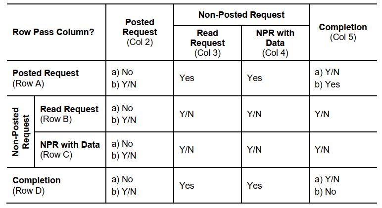
In simpler terms, in the Producer-Consumer model, the consumer side cannot use the data in a certain memory before the producer has completely written the data; and the status query register provided by the producer is not allowed to respond to the consumer's status read request before the data is fully written out. In the following diagram, the EP device is a producer, and the RC side is the consumer:
- The EP device obtains data from the source RAM and writes it to the dest RAM on the RC side using the post method, which we call PD. After writing, the EP writes a completion flag to its status register (Status Register).
- The CPU on the RC side keeps polling this status register on the EP side to check whether the produced data has been written. This polling read process is called NPS. The register data obtained from the EP side is called CPLS.
- In this process, CPLS must never be sent before any PD, or the CPU on the RC side must not respond to CPLS before the data is fully written into dest RAM. This process is called the strict Producer-Consumer model.
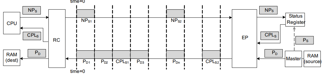
The root cause of the above problem is due to an improper business model in the device driver:
- The EP device driver and EP Firmware did not follow the protocol when using the Producer-Consumer model. When there is a gap in sending PD from the EP side to the dest RAM, and the RC side's device driver happens to send an NPS read completion flag request (including CfgRd or MemRd types), the EP side prematurely allows CPLS to be returned before PD is fully sent.
- At this time, since the RC side strictly follows the Producer-Consumer protocol model, it cannot receive CPLS without a complete PD and has no way to return with a timeout, causing the CPU waiting for CPLS to hang.
- It should also be noted that if the EP device driver does not initiate a TLP request to read the completion flag, i.e., does not want this packet to enter the strict Producer-Consumer model ordering, it should be configured as Relaxed Ordering, i.e., set the RO bit in the TLP header's Attr. Otherwise, not only may performance be degraded due to ordering, but it may also mistakenly enter the ordering rules and cause unnecessary abnormal risks.
Therefore, to break this strict model under the protocol constraints, we provide a register on the RC side that allows the ordering rules to be modified, allowing CPLS to bypass PD in the Producer-Consumer model, so that the CPU can obtain the Status Register data in advance for problem confirmation and temporary workaround. However, it should be pointed out that using our workaround below, although the RC side CPU will not hang due to CPLS being returned early during the PD gap in the Producer-Consumer model, data integrity exceptions may occur. For example, CPLS returns the completion flag early, but PDn has not been fully written into dest RAM, so the RC side CPU may get incomplete data from dest RAM, missing part of PDn. The probability of this depends on CPU speed, software delay after the driver gets the completion flag and fetches the data stream, memory latency/QoS inside the chip, and other factors. It is known that some network devices have this problem, but with the workaround and a low probability of data error rate, plus the checksum and error handling mechanism of the network protocol stack, it does not ultimately cause abnormal use. But for other devices, this cannot be guaranteed, and it depends on whether the device driver has a complete checksum and recovery mechanism. Therefore, our suggestions for EP devices that use this protocol model but cannot meet the constraints are:
- The device driver can abandon the traditional Producer-Consumer model, i.e., the method of reading registers to confirm data transmission completion, and switch to the EP side triggering MSI(-x) interrupt mechanism for notification, which is the consensus of most PCIe devices.
- If it really cannot be modified due to technical support, please confirm with the Vendor whether the non-strict Producer-Consumer mode, after adopting our workaround, has a complete error handling mechanism for data integrity in the driver, and whether it will seriously affect the business ecosystem.
1. Query the PCIe controller to obtain the dbi register base address. Take RK3588 pcie2x1l0 as an example:
pcie2x1l0: pcie@fe170000 {
           ......
           reg = <0x0 0xfe170000 0x0 0x10000>,
                 <0xa 0x40800000 0x0 0x400000>; //dbi address is the value of the first two cells high and low,
0xa40800000
           reg-names = "pcie-apb", "pcie-dbi";
}
2. Temporarily adjust the Ordering rule register to allow CPLs to bypass Pd. The register is dbi address+0x8b4:
io -4 0xa408008b4 0xff00 # 0xa40800000 + 0x8b4
3. Ordering rule register details:
_________________________________________________________________________________
__
|[0: 7] | Determines if NP can pass halted P queue. (Completion Passing Posted rule) |
|       | 0:NP can not pass P (recommended)
|
|       | 1:NP can pass P
|
|_______|________________________________________________________________________
__ |
|[8:15] | Determines if CPL can pass halted P queue.(Non-Posted Passing Posted rule) |
|       | 0: CPL can not pass P (recommended)
  |
|       | 1: CPL can pass P
  |
|_______|________________________________________________________________________
__ |
12.22 NVMe Device Abnormalities After Long-Term Operation
[186825.261896] nvme nvme0: Abort status: 0x0
[187047.435152] nvme nvme0: Abort status: 0x0
[187052.740828] nvme nvme0: I/O 256 QID 1 timeout, aborting
[187082.743811] nvme nvme0: I/O 256 QID 1 timeout, reset controller
[187092.649150] nvme nvme0: Abort status: 0x0
[187389.590726] nvme nvme0: I/O 709 QID 2 timeout, aborting
[187396.088472] nvme nvme0: Abort status: 0x0
[187419.670448] nvme nvme0: I/O 736 QID 2 timeout, aborting
[187430.034886] nvme nvme0: Abort status: 0x0
[187449.750258] nvme nvme0: I/O 736 QID 2 timeout, reset controller
Abnormalities occur in NVMe devices under stress testing. From the above log, the device status returned by the NVMe device is 0. If there is a link exception, it should return 0xf, so the link problem can be ruled out. In this case, focus on the device's operating temperature.
First, enable the NVMe thermal control configuration CONFIG_NVME_HWMON in the kernel. Then traverse the hwmon IDs to find the thermal node registered by NVMe, e.g., cat /sys/class/hwmon/hwmon8/name, and if you get nvme, it is the thermal node for the nvme device. Read the temperature sensor counts of each NVMe device cat /sys/class/hwmon/hwmon8/*input and observe the temperature changes under stress testing to see if it exceeds the rated operating temperature of the device. If the operating temperature exceeds the limit, improve the heat dissipation conditions or implement corresponding hard disk thermal control strategies in user space.
[ 3836.614828] sysrq: Show Blocked State
[ 3836.614921] task:binder:306_2   state:D stack:    0 pid:  329 ppid:     1
flags:0x04000009
[ 3836.614925] Call trace:
[ 3836.614932] __switch_to+0x118/0x148
[ 3836.614936] __schedule+0x538/0x7a4
[ 3836.614938] schedule+0x9c/0xe0
[ 3836.614940] schedule_timeout+0x8c/0xf4
[ 3836.614942] io_schedule_timeout+0x48/0x6c
[ 3836.614944] wait_for_common_io+0x7c/0x100
[ 3836.614945] wait_for_completion_io_timeout+0x10/0x1c
[ 3836.614949] submit_bio_wait+0x70/0xb4
[ 3836.614952] blkdev_issue_discard+0x88/0xd8
[ 3836.614954] blk_ioctl_discard+0x100/0x108
[ 3836.614955] blkdev_common_ioctl+0x388/0x664
[ 3836.614957] blkdev_ioctl+0x16c/0x20c
[ 3836.614959] block_ioctl+0x34/0x44
[ 3836.614962] __arm64_sys_ioctl+0x90/0xc8
[ 3836.614964] el0_svc_common+0xac/0x1ac
[ 3836.614965] do_el0_svc+0x1c/0x28
[ 3836.614968] el0_svc+0x10/0x1c
[ 3836.614970] el0_sync_handler+0x68/0xac
[ 3836.614972] el0_sync+0x160/0x180
In addition to nvme nvme0: I/O 736 QID 2 timeout, aborting, if the above print is also triggered, analyze whether a full disk format or synchronous batch deletion operation was performed before the exception, especially for large-capacity NVMe devices that are nearly full. The solution is as follows:
- Set
CONFIG_DEFAULT_HUNG_TASK_TIMEOUTto a slightly larger value, such as 120, to avoid block-mq blocking detection. - Adjust the software timeout for the NVMe protocol stack's admin queue and io queue:
--- a/drivers/nvme/host/core.c
+++ b/drivers/nvme/host/core.c
@@ -41,12 +41,12 @@ struct nvme_ns_info {
	bool is_removed;
 };
-unsigned int admin_timeout = 60;
+unsigned int admin_timeout = 120;
 module_param(admin_timeout, uint, 0644);
 MODULE_PARM_DESC(admin_timeout, "timeout in seconds for admin commands");
 EXPORT_SYMBOL_GPL(admin_timeout);
-unsigned int nvme_io_timeout = 30;
+unsigned int nvme_io_timeout = 120;
 module_param_named(io_timeout, nvme_io_timeout, uint, 0644);
13. Appendix
13.1 LTSSM State Machine
| State Code | State Descriptor | Note |
|---|---|---|
| 0x00 | S_DETECT_QUIET | No RX terminal resistor detected on the peripheral, device not working properly |
| 0x01 | S_DETECT_ACTIVE | - |
| 0x02 | S_POLL_ACTIVE | - |
| 0x03 | S_POLL_COMPLIANCE | Compliance test mode. Entered by mistake due to signal abnormality in non-test mode |
| 0x04 | S_POLL_CONFIG | - |
| 0x05 | S_PRE_DETECT_QUIET | - |
| 0x06 | S_DETECT_WAIT | - |
| 0x07 | S_CFG_LINKWD_START | - |
| 0x08 | S_CFG_LINKWD_ACEPT | Lane order detection process |
| 0x09 | S_CFG_LANENUM_WAIT | - |
| 0x0a | S_CFG_LANENUM_ACEPT | - |
| 0x0b | S_CFG_COMPLETE | Physical layer detection completed |
| 0x0c | S_CFG_IDLE | - |
| State Code | State Descriptor | Note |
|---|---|---|
| 0x0d | S_RCVRY_LOCK | Rate switching process |
| 0x0e | S_RCVRY_SPEED | - |
| 0x0f | S_RCVRY_RCVRCFG | - |
| 0x10 | S_RCVRY_IDLE | - |
| 0x20 | S_RCVRY_EQ0 | - |
| 0x21 | S_RCVRY_EQ1 | - |
| 0x22 | S_RCVRY_EQ2 | - |
| 0x23 | S_RCVRY_EQ3 | - |
| 0x11 | S_L0 | Link normal working state L0 |
| 0x12 | S_L0S | - |
| 0x13 | S_L123_SEND_EIDLE | - |
| 0x14 | S_L1_IDLE | - |
| 0x15 | S_L2_IDLE | - |
| 0x16 | S_L2_WAKE | - |
| 0x17 | S_DISABLED_ENTRY | - |
| 0x18 | S_DISABLED_IDLE | - |
| 0x19 | S_DISABLED | - |
| 0x1a | S_LPBK_ENTRY | - |
| 0x1b | S_LPBK_ACTIVE | loopback test mode, generally entered in test environment |
| 0x1c | S_LPBK_EXIT | - |
| 0x1d | S_LPBK_EXIT_TIMEOUT | - |
| 0x1e | S_HOT_RESET_ENTRY | Peripheral initiates its hot reset process |
| 0x1f | S_HOT_RESET | - |
13.2 Debugfs Exported Information Interpretation Table
| Event Symbol | Meaning |
|---|---|
| EBUF Overflow | - |
| EBUF Underrun | - |
| Decode Error | Packet decoding error, signal abnormality |
| Running Disparity Error | Polarity deviation error, 8bit/10bit encoding 0 and 1 ratio imbalance, Gen2 signal abnormality |
| SKP OS Parity Error | SKP sequence parity error, Gen3 signal abnormality |
| SYNC Header Error | Asynchronous packet header error, signal problem |
| CTL SKP OS Parity Error | Control SKP sequence parity error, Gen3 signal abnormality |
| Detect EI Inference | Detected signal crosstalk |
| Receiver Error | Receiver error |
| Rx Recovery Request | RX signal received peripheral request, enters recovery state for signal correction |
| N_FTS Timeout | Peripheral's n_fts not up to standard, L0s returns to L0 abnormally entering recovery state |
| Framing Error | Frame format decoding error, signal abnormality |
| Deskew Error | deskew error, signal abnormality |
| BAD TLP | Received bad TLP packet |
| LCRC Error | link CRC, signal abnormality |
| BAD DLLP | Bad DLLP packet, signal abnormality |
| Replay Number Rollover | Too many retransmitted packets accumulated, replay buffer overflowed |
| Replay Timeout | Retransmission timeout for error packets |
| Rx Nak DLLP | Received DLLP from downstream and access was refused |
| Tx Nak DLLP | DLLP sent to downstream was refused |
| Retry TLP | Number of retransmitted TLP packets, can indicate error rate |
| FC Timeout | Flow control update timeout |
| Poisoned TLP | Reports a bad TLP type, possibly due to link reasons or RAM bit flips |
| ECRC Error | end CRC, signal abnormality |
| Unsupported Request | Received unsupported TLP request, possibly access to peripheral was refused |
| Completer Abort | Device received a request from RC, but an internal error occurred and the access request was terminated |
| Event Symbol | Meaning |
|---|---|
| Completion Timeout | Timeout when reading peripheral-related resources, TLP return timeout |
| Common event signal | Read the current controller's PM mode |
13.3 Error Injection Configuration Comparison Table
| Group No. | Group Description | Type No. | Type Meaning |
|---|---|---|---|
| 0 | CRC Error | 0x0 | TLP LCRC error packet |
| 0 | CRC Error | 0x1 | 16b CRC of ACK/NAK DLLP error packet |
| 0 | CRC Error | 0x2 | 16b CRC of Update-FC DLLP error packet |
| 0 | CRC Error | 0x3 | TLP ECRC error packet |
| 0 | CRC Error | 0x4 | TLP FCRC error packet (128b/130bit encoding) |
| 0 | CRC Error | 0x5 | TX polarity error TSOS (128b/130bit encoding) |
| 0 | CRC Error | 0x6 | TX polarity error SKPOS (128b/130bit encoding) |
| 0 | CRC Error | 0x8 | RX LCRC error packet |
| 0 | CRC Error | 0xb | RX ECRC error packet |
| Group No. | Group Description | Type No. | Type Meaning |
|---|---|---|---|
| 1 | Packet Number Sequence Error | 0x0 | TLP SEQ# error |
| 1 | Packet Number Sequence Error | 0x1 | DLLP SEQ# error ACK_NAK_DLLP |
| Group No. | Group Description | Type No. | Type Meaning |
|---|---|---|---|
| 2 | DLLP Error | 0x0 | Block transmission of DLLP ACK/NAK packet[1] |
| 2 | DLLP Error | 0x1 | Block transmission of Update FC DLLP packet[1] |
| 2 | DLLP Error | 0x2 | Always send NAK DLLP packet[1] |
| Group No. | Group Description | Type No. | Type Meaning |
|---|---|---|---|
| 3 | Symbol Error | 0x0 | Invert sync header (128bit/130bit encoding) |
| 3 | Symbol Error | 0x1 | TS1 order set error |
| 3 | Symbol Error | 0x2 | TS2 order set error |
| 3 | Symbol Error | 0x3 | FTS order set error |
| 3 | Symbol Error | 0x4 | E-idle order set error |
| 3 | Symbol Error | 0x5 | END/EDB symbol error |
| 3 | Symbol Error | 0x6 | STP/SDP symbol error |
| 3 | Symbol Error | 0x7 | SKP order set error |
| Group No. | Group Description | Type No. | Type Meaning |
|---|---|---|---|
| 4 | Flow Control FC Error | 0x0 | Posted TLP header credit |
| 4 | Flow Control FC Error | 0x1 | Non-Posted TLP header credit |
| 4 | Flow Control FC Error | 0x2 | Completion TLP header credit |
| 4 | Flow Control FC Error | 0x4 | Posted TLP Data credit |
| 4 | Flow Control FC Error | 0x5 | Non-Posted TLP Data credit |
| 4 | Flow Control FC Error | 0x6 | Completion TLP data credit |
| Group No. | Group Description | Type No. | Type Meaning |
|---|---|---|---|
| 5 | Special TLP Error | 0x0 | Generate ACK DLLP as NAK DLLP |
| 5 | Special TLP Error | 0x1 | Generate invalid TLP packet, original packet enters retry process |
| Group No. | Group Description | Type No. | Type Meaning |
|---|---|---|---|
| 6 | Packet Header Check Error | 0x0 | Generate TLP header error |
| 6 | Packet Header Check Error | 0x1 | Generate error in the first group of four dwords in TLP prefix |
| 6 | Packet Header Check Error | 0x2 | Error in the second group of dwords in TLP prefix |
[1] Does not depend on counting to zero to stop, requires manual command to stop
13.4 PCIe TX De-emphasis Preset Value Comparison Table
| Preset Number | Preshoot(dB) | De-emphasis(dB) |
|---|---|---|
| P0 | 0 | -6.0 ± 1.5 dB |
| P1 | 0 | -3.5 ± 1 dB |
| P2 | 0 | -4.4 ± 1.5 dB |
| P3 | 0 | -2.5 ± 1 dB |
| P4 | 0 | 0 |
| P5 | 1.9 ± 1 dB | 0 |
| P6 | 2.5 ± 1 dB | 0 |
| P7 | 3.5 ± 1 dB | -6.0 ± 1.5 dB |
| P8 | 3.5 ± 1 dB | -3.5 ± 1 dB |
| P9 | 3.5 ± 1 dB | 0 |
| P10 | 0 | x |
13.5 Development Resource Access Address
After obtaining redmine permission, you can directly access https://redmine.rock-chips.com/documents/107 to obtain the various materials mentioned above.
13.6 Detailed PCIe Address Space Configuration
For detailed configuration of PCIe address space in DTS, refer to the following link for interpretation or modification: https://elinux.org/Device_Tree_Usage#PCI_Host_Bridge
13.7 M.2 Interface Hardware
Key B+M gold fingers can use key B or key M adapter slots, key A+E gold fingers can use key A or key E adapter slots. For other types of gold finger boards, please strictly select the corresponding type of adapter slot according to the interface.
13.8 Board-Level Configurable Timing
| Adjustable Time | dts property | Description (Linux kernel stage) |
|---|---|---|
| Power Stable | rockchip,vpcie3v3-supply | This property is configured in the power node referenced by the vpcie3v3-supply property of the PCIe node |
| Tpvperl | rockchip,perst-inactive-ms | This property is configured in the PCIe node. If not configured, the default is 200ms, effective at boot |
| Tpvperl | rockchip,s2r-perst-inactive-ms | This property is configured in the PCIe node. If not configured, the default is the same as rockchip,perst-inactive-ms, effective during suspend/resume |
| out of electrical idle | rockchip,wait-for-link-ms | This property is configured in the PCIe node. If not configured, the default is 1ms, used to wait before each link initiation |
13.9 PCIe Controller QoS Adjustment Registers in Each SoC
The register command examples in the table below are configured to the highest allowed priority. Please adjust as appropriate according to test results.
| Chip | Controller | Register Command | |
|---|---|---|---|
| RK1808 | pcie0 | io -4 0xfe880008 | 0x303 |
| RK3528 | pcie2x1 | io -4 0xff280188 | 0x404 |
| RK3562 | pcie2x1 | io -4 0xfeea0008 | 0x404 |
| RK3562 | pcie2x1 | io -4 0xfe190008 | 0x80000303 |
| RK3566 | pcie3x1 | io -4 0xfe190088 | 0x80000303 |
| RK3568 | pcie3x2 | io -4 0xfe190108 | 0x80000303 |
| RK3576 | pcie0 | io -4 0x27f0a008 | 0x303 |
| RK3576 | pcie1 | io -4 0x27f0a088 | 0x303 |
| RK3588 | PCIe1L0/1/2 | io -4 0xfdf3a008 | 0x404 |
| RK3588 | PCIe3x4 PCIe3x2 | io -4 0xfdf3a208 | 0x404 |