
DP
Preface
This article mainly introduces the usage and debugging methods of the DP interface on the Rockchip platform.
Product Versions
| Chip Name | Kernel Version |
|---|---|
| RK3576 | LINUX Kernel 6.1 |
| RK3588 | LINUX Kernel 5.10/6.1 |
Target Audience
This document (guide) is mainly intended for the following engineers:
Technical Support Engineers
Software Development Engineers
1. Introduction to DisplayPort on Rockchip Platform
1.1 Features
The DP interface feature parameters of Rochchip RK3576 and RK3588 are as follows:
| Feature | RK3576 | RK3588 |
|---|---|---|
| Version | 1.4a | 1.4a |
| SST | Support | Support |
| MST | Support | Not support |
| DSC | Not support | Not support |
| Max resolution | 4K@120Hz | 8K@30Hz |
| Main-Link lanes | 1/2/4 lanes | 1/2/4 lanes |
| Main-Link rate | 8.1/5.4/2.7/1.62 Gbps/lane | 8.1/5.4/2.7/1.62 Gbps/lane |
| AUX_CH | 1M | 1M |
| Color Format | RGB/YUV444/YUV422/YUV420 | RGB/YUV444/YUV422/YUV420 |
| Color Depth | 8/10 bit(6bit just for RGB) | 8/10 bit(6bit just for RGB) |
| Display Split Mode | Support | Support |
| HDCP | HDCP2.2/HDCP1.3 | HDCP2.2/HDCP1.3 |
| Type-C support | DP Alternate Mode | DP Alternate Mode |
| I2S | Support | Support |
| SPDIF | Support | Support |
| HDR | Support | Support |
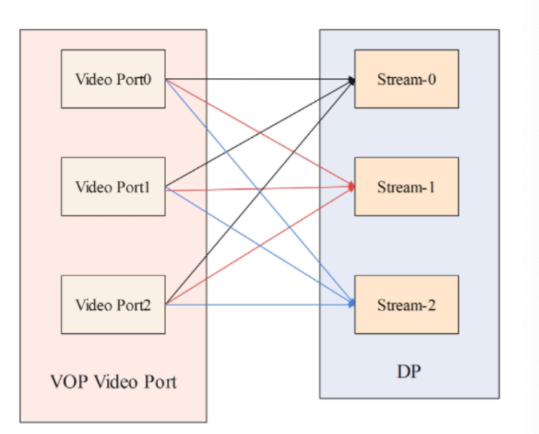
RK3576 has only one physical DP interface, but in MST mode it can internally accept 3 display data streams (to distinguish physical interfaces, use Stream-0, Stream-1, Stream-2). The maximum output capability of each stream is as follows:
| DP Stream Channel | max width | max height | max pixel clock |
|---|---|---|---|
| Stream-0 | 4096 | 2160 | 1188MHz |
| Stream-1 | 2560 | 1440 | 300MHz |
| Stream-2 | 1920 | 1080 | 150MHz |
1.2 DP and VOP Connection Relationship
RK3576's VOP has three Video Ports and one DP controller. In MST mode, the DP controller supports receiving up to 3 display data streams from the VOP. Stream-0/1/2 can all receive display data from Video Port0/1/2. When working in SST mode, only Stream-0 in the DP controller can be used. In MST mode, Stream-0/1/2 can all be used.
RK3588's VOP has four Video Ports and two DP controllers, among which only Video Port 0/1/2 can output to DP0/1, as shown below.
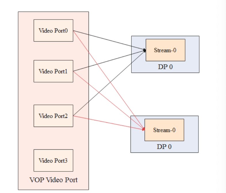
For RK3588, the two DP interfaces do not support MST mode, and can only receive one display data stream Stream-0 internally. For such platforms that do not support MST, by default the Video Port output is output to the Stream-0 of the DP interface.
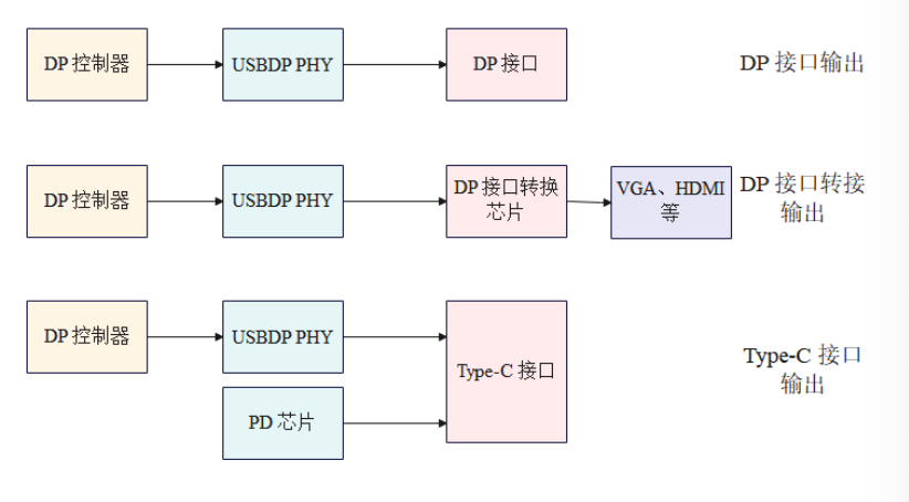
1.3 DP Output
According to different application scenarios, different DP output methods can be designed: Type-C interface output, standard DP interface output, or output through other adapter chips.
RK3576 can connect up to 3 monitors in MST mode, and can be daisy-chained through MST monitors as shown below:
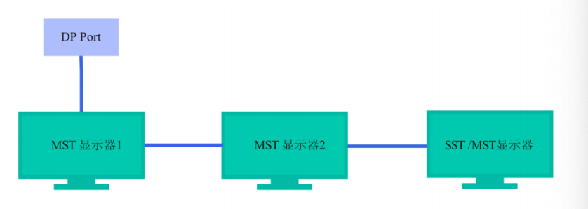
For monitors connected in a daisy chain, only the last monitor can be an SST monitor, others need to be MST monitors.
Another way is to connect through an MST HUB, as shown below:
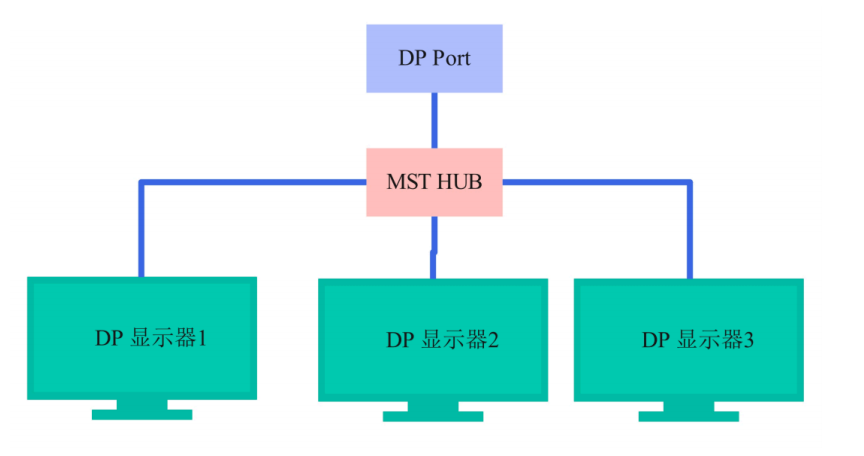
When connecting through an MST HUB, the DP monitor can be either an SST monitor or an MST monitor.
1.4 Code Paths
U-Boot driver code:
drivers/video/drm/dw-dp.c
drivers/phy/phy-rockchip-usbdp.c
Kernel driver code:
drivers/gpu/drm/rockchip/dw-dp.c
drivers/phy/rockchip/phy-rockchip-usbdp.c
RK3576 reference DTS configuration:
arch/arm64/boot/dts/rockchip/rk3576-evb1.dtsi
arch/arm64/boot/dts/rockchip/rk3576-test2.dtsi
RK3588 reference DTS configuration:
arch/arm64/boot/dts/rockchip/rk3588-evb1-lp4.dtsi
arch/arm64/boot/dts/rockchip/rk3588-evb2-lp4.dtsi
arch/arm64/boot/dts/rockchip/rk3588-evb3-lp5.dtsi
arch/arm64/boot/dts/rockchip/rk3588-nvr-demo.dtsi
1.5 Driver Loading
Check the following log to determine whether the driver has finished loading:
RK3576:
 [1.991964] rockchip-drm display-subsystem: bound 27e40000.dp (ops 0xffffffc0094a1570) //DP driver loaded
RK3588:
 [2.472282] rockchip-drm display-subsystem: bound fde50000.dp (ops dw_dp_component_ops) //DP0 driver loaded
 [2.472319] rockchip-drm display-subsystem: bound fde60000.dp (ops dw_dp_component_ops) //DP1 driver loaded
2. Feature Configuration
For the DP interface, there are differences in the basic DTS node configuration between platforms that support MST and those that do not.
For platforms that do not support MST, such as RK3588, a DP controller only supports one DP output, and only one ports subnode needs to be defined to describe the display path supported by this DP. The DP node is described as follows:
dp0: dp@fde50000 {
    compatible = "rockchip,rk3588-dp";
    ...

    ports {
          #address-cells = <1>;
          #size-cells = <0>;

          port@0 {
              reg = <0>;
              #address-cells = <1>;
              #size-cells = <0>;

              dp0_in_vp0: endpoint@0 {
                     reg = <0>;
                     remote-endpoint = <&vp0_out_dp0>;
                     status = "disabled";
              };
                dp0_in_vp1: endpoint@1 {
                     reg = <1>;
                     remote-endpoint = <&vp1_out_dp0>;
                     status = "disabled";
                };

                dp0_in_vp2: endpoint@2 {
                     reg = <2>;
                     remote-endpoint = <&vp2_out_dp0>;
                     status = "disabled";
                };
           };
     ...
     };
};
For platforms that support MST, such as RK3576, a DP controller needs to support 3 display data stream outputs, and one ports node cannot describe multiple DP channel display paths, so multiple subnodes are needed, configured as follows:
dp: dp@27e40000 {
     compatible = "rockchip,rk3576-dp";
     ...
     dp0: dp0 {
           status = "disabled";

           ports {
                #address-cells = <1>;
                #size-cells = <0>;

                port@0 {
                     reg = <0>;
                     #address-cells = <1>;
                     #size-cells = <0>;

                     dp0_in_vp0: endpoint@0 {
                           reg = <0>;
                           remote-endpoint = <&vp0_out_dp0>;
                           status = "disabled";
                     };

                     dp0_in_vp1: endpoint@1 {
                           reg = <1>;
                           remote-endpoint = <&vp1_out_dp0>;
                           status = "disabled";
                     };

                     dp0_in_vp2: endpoint@2 {
                           reg = <2>;
                           remote-endpoint = <&vp2_out_dp0>;
                           status = "disabled";
                     };
                };
           };
     };
dp1: dp1 {
    status = "disabled";

    ports {
         #address-cells = <1>;
         #size-cells = <0>;

         port@0 {
              reg = <0>;
              #address-cells = <1>;
              #size-cells = <0>;

              dp1_in_vp0: endpoint@0 {
                    reg = <0>;
                    remote-endpoint = <&vp0_out_dp1>;
                    status = "disabled";
              };

              dp1_in_vp1: endpoint@1 {
                    reg = <1>;
                    remote-endpoint = <&vp1_out_dp1>;
                    status = "disabled";
              };

              dp1_in_vp2: endpoint@2 {
                    reg = <2>;
                    remote-endpoint = <&vp2_out_dp1>;
                    status = "disabled";
              };
         };
    };
};

dp2: dp2 {
    status = "disabled";

    ports {
         #address-cells = <1>;
         #size-cells = <0>;
         port@0 {
              reg = <0>;
              #address-cells = <1>;
              #size-cells = <0>;

              dp2_in_vp0: endpoint@0 {
                    reg = <0>;
                    remote-endpoint = <&vp0_out_dp2>;
                    status = "disabled";
              };

              dp2_in_vp1: endpoint@1 {
                    reg = <1>;
                    remote-endpoint = <&vp1_out_dp2>;
                    status = "disabled";
              };
                    dp2_in_vp2: endpoint@2 {
                         reg = <2>;
                         remote-endpoint = <&vp2_out_dp2>;
                         status = "disabled";
                    };
               };
          };
     };
};
The above dp0/1/2 subnodes respectively describe the display paths that Stream-0/1/2 in the DP controller can support.
Compared with the DTS configuration, platforms that support MST have an extra layer of DP channel subnodes.
2.1 Enabling DP
DP and USB3.0 share a PHY. The configuration of PHY lanes varies according to the interface: Type-C mode and non-Type-C mode.
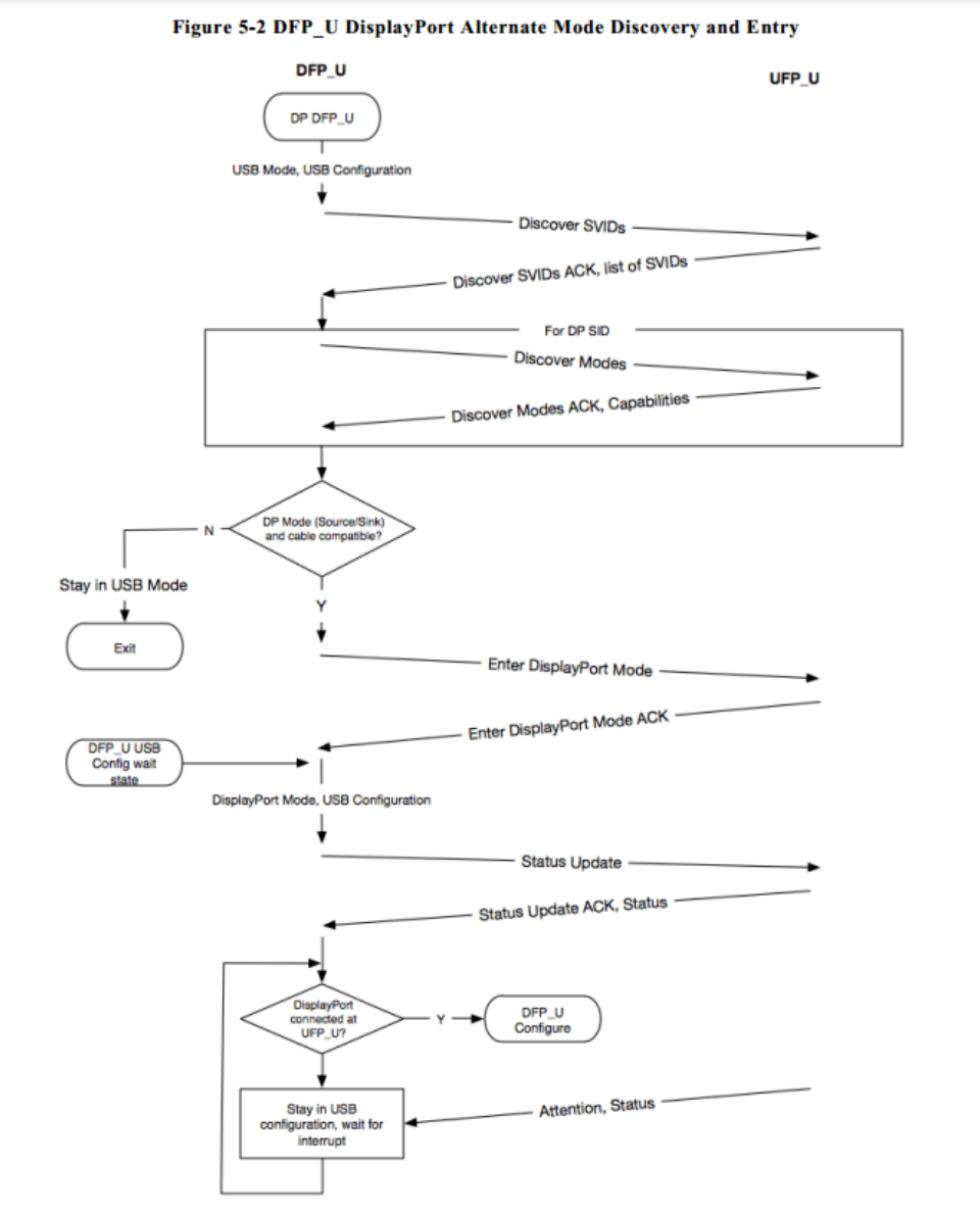
2.1.1 DP Alt Mode (Type-C)
According to the DisplayPort Alt Mode protocol, communication with the monitor is carried out through the PD (Power Delivery) state machine, lane mapping, and HPD information transmission. The process of entering DP Mode through the PD protocol and transmitting HPD information through the attention command is mainly as shown below.
For platforms that do not support MST, such as RK3588, the configuration is as follows:
&dp0 {
     status = "okay";
};

&dp0_in_vp2 {
     status = "okay";
};
In the above configuration, DP0 interface is enabled and DP0 is bound to Video Port2 of the VOP. This is just a reference configuration. In actual use, you can enable DP0 or DP1 as needed, and bind DP0 or DP1 to the desired Video Port (0/1/2).
For platforms that support MST, such as RK3576, the configuration is as follows:
&dp {
     status = "okay";
};

&dp0 {
     status = "okay";
};

&dp0_in_vp2 {
     status = "okay";
};
As you can see, for platforms that support MST, you need to enable the DP device node, the DP Stream channel to be enabled, and the Video Port on the VOP to which the channel is to be bound. In the above configuration, Stream-0 of the DP interface is enabled and Stream-0 is bound to Video Port2 of the VOP.
Note that for platforms that support MST, since SST mode must use DP Stream-0, the dp0 node must be enabled. dp1 and dp2 are configured as needed.
PHY configuration is as follows, with no difference between platforms that support MST and those that do not. Refer to the configuration of RK3588 usbdp phy0:
&usbdp_phy0 {
     status = "okay";
     orientation-switch;
     /* DP related config */
     svid = <0xff01>;
     sbu1-dc-gpios = <&gpio4 RK_PA6 GPIO_ACTIVE_HIGH>;
     sbu2-dc-gpios = <&gpio4 RK_PA7 GPIO_ACTIVE_HIGH>;
     /* DP related config */

     port {
          #address-cells = <1>;
          #size-cells = <0>;
          usbdp_phy0_orientation_switch: endpoint@0 {
                reg = <0>;
                remote-endpoint = <&usbc0_orien_sw>;
          };

          /* DP related config */
          usbdp_phy0_dp_altmode_mux: endpoint@1 {
                reg = <1>;
                remote-endpoint = <&dp_altmode_mux>;
          };
          /* DP related config */
     };
};
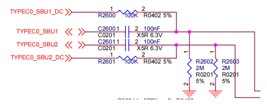
sbu1-dc-gpios and sbu2-dc-gpios:
The SBU1 and SBU2 pins of Type-C are multiplexed with the AUX_CH of DP. When Type-C is inserted normally, AUX_CH_P is multiplexed with SBU1, and AUX_CH_N is multiplexed with SBU2. When Type-C is inserted reversely, AUX_CH_P is multiplexed with SBU2, and AUX_CH_N is multiplexed with SBU1. According to the DP protocol, AUX_CH_P needs to be configured as pull-down, and AUX_CH_N needs to be configured as pull-up. The multiplexing configuration of AUX_CH_N and AUX_CH_P is different for different insertion states (normal and reverse) of Type-C. In the RK solution, two GPIOs are used to control the pull-up and pull-down states of SBU1 and SBU2 respectively, i.e., sbu1-dc-gpios and sbu2-dc-gpios in the dts. Therefore, when configuring the PHY, you need to configure sbu1-dc-gpios and sbu2-dc-gpios (when actually configuring these two GPIOs, refer to the schematic diagram of the hardware design, such as TYPEC0_SBU1_DC and TYPEC0_SBU2_DC in the figure below). The PHY driver will adjust the GPIO output level according to the current normal or reverse insertion state of Type-C.
svid:
For DP, it is a fixed value of 0xff01.
Type-C interface requires lane and HPD status configuration through Type-C CC detection and PD negotiation, so a PD chip also needs to be configured:
&i2c2 {
     status = "okay";

     usbc0: fusb302@22 {
          compatible = "fcs,fusb302";
          reg = <0x22>;
          interrupt-parent = <&gpio3>;
          interrupts = <RK_PB4 IRQ_TYPE_LEVEL_LOW>;
          pinctrl-names = "default";
          pinctrl-0 = <&usbc0_int>;
          vbus-supply = <&vbus5v0_typec>;
          status = "okay";

          ports {
               #address-cells = <1>;
               #size-cells = <0>;

               port@0 {
                    reg = <0>;
                    usbc0_role_sw: endpoint@0 {
                          remote-endpoint = <&dwc3_0_role_switch>;
                    };
               };
          };

          usb_con: connector {
               compatible = "usb-c-connector";
               label = "USB-C";
               data-role = "dual";
               power-role = "dual";
               try-power-role = "sink";
               op-sink-microwatt = <1000000>;
               sink-pdos =
                    <PDO_FIXED(5000, 1000, PDO_FIXED_USB_COMM)>;
               source-pdos =
                    <PDO_FIXED(5000, 3000, PDO_FIXED_USB_COMM)>;

               /* DP related config */
               altmodes {
                    #address-cells = <1>;
                    #size-cells = <0>;

                    altmode@0 {
                         reg = <0>;
                         svid = <0xff01>;
                         vdo = <0xffffffff>;
                    };
               };
               /* DP related config */

               ports {
                    #address-cells = <1>;
                    #size-cells = <0>;

                    port@0 {
                         reg = <0>;
                         usbc0_orien_sw: endpoint {
                               remote-endpoint = <&usbdp_phy0_orientation_switch>;
                         };
                    };

                    /* DP related config */
                    port@1 {
                         reg = <1>;
                         dp_altmode_mux: endpoint {
                               remote-endpoint = <&usbdp_phy0_dp_altmode_mux>;
                         };
                    };
                    /* DP related config */
               };
          };
     };
};
In the altmode@0 node, svid is fixed to 0xff01, and vdo is fixed to 0xffffffff.
Note: Currently supported PD chips are fusb302 and hub311. The driver for fusb302 is /drivers/usb/typec/tcpm/fusb302.c, and for hub311 is /drivers/usb/typec/tcpm/tcpci_husb311.c.
2.1.2 DP Legacy Mode
For non-Type-C interface output, whether it is a DP interface or output through other adapter chips, the configuration process is basically the same, and HPD Pin must be configured. When actually assigning IO pins, you can use the dedicated DP_HPD pin, which is configured according to IOMUX, or you can use a regular GPIO for detection.
For platforms that do not support MST, such as RK3588, when using the DP_HPD Pin, the configuration is as follows:
&dp1 {
     pinctrl-0 = <&dp1m2_pins>;
     pinctrl-names = "default";
     status = "okay";
};

&dp1_in_vp2 {
     status = "okay";
};
When using a regular GPIO for HPD detection, the configuration is as follows:
&dp1 {
     pinctrl-names = "default";
     pinctrl-0 = <&dp1_hpd>;
     hpd-gpios = <&gpio1 RK_PB5 GPIO_ACTIVE_HIGH>;
     status = "okay";
};

&dp1_in_vp2 {
     status = "okay";
};

&pinctrl {
     dp {
            dp1_hpd: dp1-hpd {
                 rockchip,pins = <1 RK_PB5 RK_FUNC_GPIO &pcfg_pull_down>;
            };
     };
};
For platforms that support MST, such as RK3576, when using the DP_HPD Pin, the configuration is as follows:
&dp {
     pinctrl-0 = <&dp1m2_pins>;
     pinctrl-names = "default";
     status = "okay";
};

&dp0 {
     status = "okay";
};

&dp0_in_vp2 {
     status = "okay";
};
When using a regular GPIO for HPD detection, the configuration is as follows:
&dp {
     pinctrl-names = "default";
     pinctrl-0 = <&dp_hpd>;
     hpd-gpios = <&gpio1 RK_PB5 GPIO_ACTIVE_HIGH>;
     status = "okay";
};

&dp0 {
     status = "okay";
};

&dp0_in_vp2 {
     status = "okay";
};

&pinctrl {
     dp {
            dp_hpd: dp-hpd {
                 rockchip,pins = <1 RK_PB5 RK_FUNC_GPIO &pcfg_pull_down>;
            };
     };
};
In the above configurations for platforms that support and do not support MST, the HPD configuration belongs to the entire DP interface and is configured under the device node.
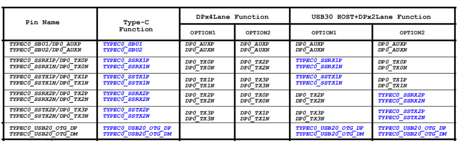
DP and USB 3.0 share a PHY. When DP is output through a non-Type-C interface, you need to specify the lane configuration for DP and the corresponding lane number in the DTS. The PHY lane can be configured in 2-lane or 4-lane mode.
The physical numbering of the PHY lane interface is as shown below:

For DP configured with 4 lanes, the dtsi configuration attribute is as follows:
rockchip,dp-lane-mux = <x x x x>;
For DP configured with 2 lanes, the dtsi configuration attribute is as follows:
rockchip,dp-lane-mux = <x x>;
Where the index is the DP lane, and the value is the PHY lane. Whether 2-lane or 4-lane configuration, hardware design generally uses one of the following two options: OPTION1 or OPTION2.
For DP 4-lane OPTION1 mapping relationship is as follows:
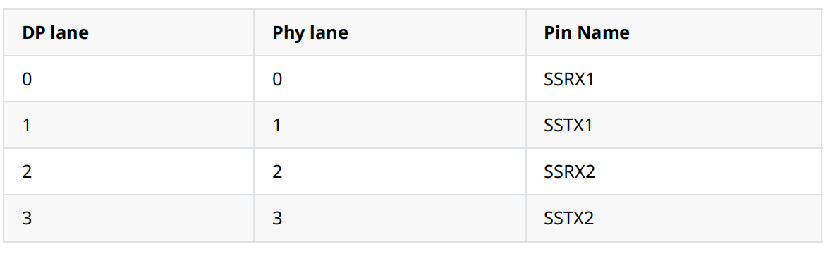
Where DP lane is the serial number of the DP lane. The dts configuration is as follows:
&usbdp_phy1 {
rockchip,dp-lane-mux = <0 1 2 3>;
status = "okay";
};
For DP 4-lane OPTION2 mapping relationship is as follows:

Where DP lane is the serial number of the DP lane. The dts configuration is as follows:
&usbdp_phy1 {
rockchip,dp-lane-mux = <2 3 0 1>;
status = "okay";
};
For DP 2-lane OPTION1 mapping relationship is as follows:
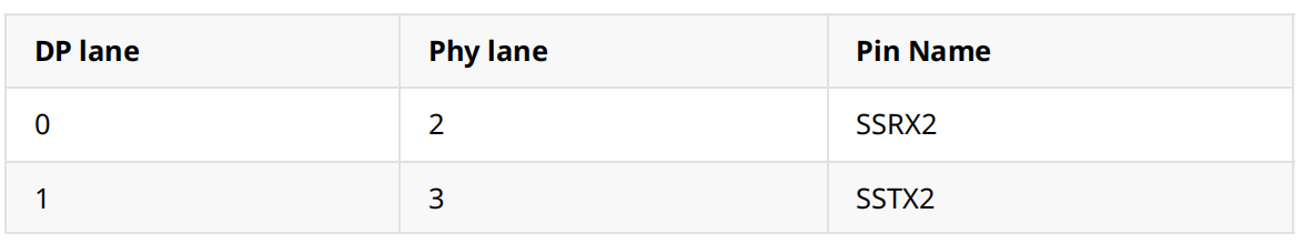
DP 2-lane configuration is as follows:
&usbdp_phy1 {
rockchip,dp-lane-mux = <2 3>;
status = "okay";
};
For DP 2-lane OPTION2 mapping relationship is as follows:
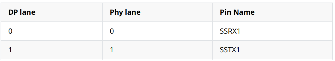
DP 2-lane configuration is as follows:
&usbdp_phy1 {
rockchip,dp-lane-mux = <0 1>;
status = "okay";
};
2.2 DP Connects to Panel Peripheral
When using the DP interface to connect to an eDP Panel, eDP-specific features such as PSR, Multi-SST, and ALPM are not supported. The panel configuration can be referred to as follows and adjusted according to the actual hardware design:
For platforms that do not support MST, such as RK3588, the configuration is as follows:
/{
...
    panel-edp {
        compatible = "simple-panel";
        backlight = <&backlight>;
        power-supply = <&vcc3v3_lcd_edp>;
        prepare-delay-ms = <120>;
enable-delay-ms = <120>;
        unprepare-delay-ms = <120>;
        disable-delay-ms = <120>;
        width-mm = <120>;
        height-mm = <160>;
        panel-timing {
            clock-frequency = <200000000>;
            hactive = <1536>;
            vactive = <2048>;
            hfront-porch = <12>;
            hsync-len = <16>;
            hback-porch = <48>;
            vfront-porch = <8>;
            vsync-len = <4>;
            vback-porch = <8>;
            hsync-active = <0>;
            vsync-active = <0>;
            de-active = <0>;
            pixelclk-active = <0>;
};
        port {
            panel_in_edp: endpoint {
                remote-endpoint = <&dp0_out>;
            };
}; };
... };
&dp0 {
    force-hpd;
    status = "okay";
};
&dp0_in_vp2 {
    status = "okay";
};
&dp0_out {
    remote-endpoint = <&panel_in_edp>;
};
&usbdp_phy0 {
    rockchip,dp-lane-mux = <0 1 2 3>;
    status = "okay";
};
For platforms that support MST, such as RK3576, the configuration is as follows:
/ {
    ...
    panel-edp {
        compatible = "simple-panel";
        backlight = <&backlight>;
        power-supply = <&vcc3v3_lcd_edp>;
        prepare-delay-ms = <120>;
        enable-delay-ms = <120>;
        unprepare-delay-ms = <120>;
        disable-delay-ms = <120>;
        width-mm = <120>;
        height-mm = <160>;
        panel-timing {
            clock-frequency = <200000000>;
            hactive = <1536>;
            vactive = <2048>;
            hfront-porch = <12>;
            hsync-len = <16>;
            hback-porch = <48>;
            vfront-porch = <8>;
            vsync-len = <4>;
            vback-porch = <8>;
            hsync-active = <0>;
            vsync-active = <0>;
            de-active = <0>;
            pixelclk-active = <0>;
        };
        port {
            panel_in_edp: endpoint {
                remote-endpoint = <&dp0_out>;
            };
        };
    };
    ...
};
&dp0 {
    force-hpd;
    status = "okay";
};
&dp0 {
    status = "okay";
    ports {
        port@1 {
reg = <1>;
            dp0_out_panel: endpoint {
                remote-endpoint = <&panel_in_edp>;
};
};
};
};
&dp0_in_vp2 {
    status = "okay";
};
&usbdp_phy {
    rockchip,dp-lane-mux = <0 1 2 3>;
    status = "okay";
};
In the above configuration, the force-hpd attribute in the dp0 node, when configured, makes the driver assume that the eDP panel is always connected. This attribute is not mandatory. Whether to configure the force-hpd attribute depends on whether the specific panel has an HPD pin, whether HPD is pulled high, and whether there are timing requirements for AUX access. If the panel requires AUX access only after HPD is pulled high, do not configure the force-hpd attribute, otherwise, there may be a situation where AUX is accessed before HPD is pulled high, causing AUX access to fail. If you still need to configure the HPD pin, refer to the HPD configuration in 1.2.1 DP Legacy Mode.
The panel-timing configures the currently supported timing. If the eDP panel does not have EDID, or the timing read from EDID is inaccurate, you need to configure the panel-timing node. Otherwise, you can omit it and obtain timing directly by reading EDID.
The power-on/off sequence and backlight should be configured according to the specific screen and hardware design.
2.3 DP Boot Logo
After configuring the boot logo, if a DP monitor is connected before boot, the logo will be displayed during the U-Boot stage. Otherwise, the application image will only be visible after the system starts. The configuration to add DP boot logo support is as follows:
&route_dp0 {
    status = "okay";
    connect = <&vp2_out_dp0>;
};
Note that the connect property here configures DP to bind to VOP Port2 during the U-Boot stage, so the dtsi configuration must allow DP to bind to VOP Port2.
&dp0_in_vp2 {
    status = "okay";
};
Note:
- Currently, DP boot logo is not supported on Type-C interfaces.
- For platforms supporting MST, the boot LOGO is only supported in SST mode.
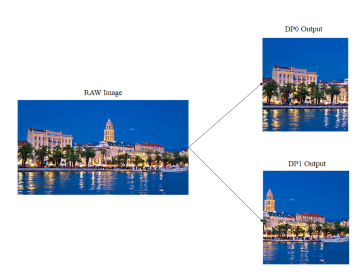
2.4 DP connector-split mode
DP connector-split mode is shown in the figure below: an image is split into left and right halves, which are transmitted to the monitor via DP0/DP1 interfaces. In the diagram, DP0 is the left half, and DP1 is the right half.
Configuration is as follows:
&dp0 {
    split-mode;
    status = "okay";
};
&dp0_in_vp2 {
    status = "okay";
};
&dp1 {
    status = "okay";
};
Add the split-mode property to the DP node acting as the left half, and bind the output Video Port. In the above configuration, DP0 is the left screen, DP1 is the right screen. In Split Mode, the two DPs act as one connector; only when both DP0 and DP1 are connected will the connector be active and display output. If either DP interface is disconnected, the connector is considered disconnected and will not output. In this mode, both DP interfaces output the same timing; it is recommended to use two identical monitors.
In user space, only one DP connector will be seen via modetest or by checking the state node (cat /sys/kernel/debug/dri/0/state).
To display the U-boot logo in split mode (e.g., DP0 as the left half), refer to the following configuration:
&route_dp0 {
 split-mode;
 status = "okay";
 connect = <&vp2_out_dp0>;
};
&route_dp1 {
 status = "disabled";
}
Note: RK3576 only has one interface and does not support this connector-split mode. Support for split mode on RK3576 will be added later. If you need split-mode functionality on RK3576, please contact Rockchip.
2.5 HDR
HDR is supported by default in SST mode; no driver configuration is required. HDR is not supported in MST mode.
2.6 HDCP
The DP driver implements HDCP functionality based on the DRM framework. To use HDCP, users need to call the DRM interface in userspace.
- HDCP1.3 is supported by default in the DP driver; no configuration is required. For HDCP Key burning, refer to "Rockchip_RK3588_Developer_Guide_HDCP_CN".
- HDCP2.2 is controlled by a separate HDCP2 controller. To enable the HDCP2 controller, configure the dts.
On RK3588, DP0/DP1 are connected to HDCP0, as shown below:
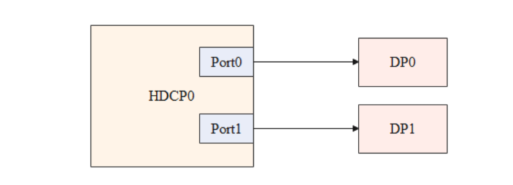
To enable DP HDCP2.2, enable the following node:
&hdcp0 {
 status = "okay";
};
On RK3576, DP is connected to HDCP1, as shown below:
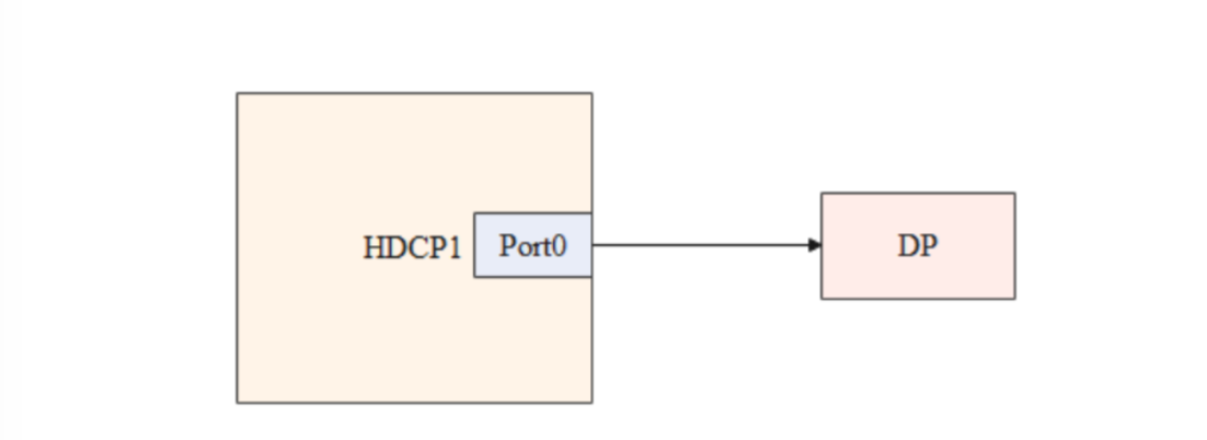
To enable DP HDCP2.2, enable the following node:
&hdcp1 {
    status = "okay";
};
In addition to driver configuration, using HDCP2.2 also requires enabling the userspace HDCP2.2 application and generating firmware for the HDCP controller. Refer to "Rockchip_RK3588_Developer_Guide_HDCP_CN".
3. Common DEBUG Methods
3.1 Check connector status
In the /sys/class/drm directory, you can see the cards registered by the driver. In the following output, card0-DP-1 and card0-DP-2 are DP display devices.
rk3588_s:/ # ls /sys/class/drm/
card0       card0-DP-2   card0-HDMI-A-1 card0-Writeback-1 renderD128 version
card0-DP-1 card0-DSI-1 card0-HDMI-A-2 card1             renderD129
Take card0-DP-1 as an example, its directory contains:
rk3588_s:/ # ls /sys/class/drm/card0-DP-1/
device dpms edid enabled modes power status subsystem uevent
Check enable status:
rk3588_s:/ # cat /sys/class/drm/card0-DP-1/enabled
disabled
Check connection status:
rk3588_s:/ # cat /sys/class/drm/card0-DP-1/status
disconnected
modes: list of supported resolutions:
rk3588_s:/ # cat /sys/class/drm/card0-DP-1/modes
1440x900
1280x1024
1280x1024
1280x960
1152x864
1024x768
1024x768
832x624
800x600
800x600
640x480
640x480
720x400
edid: device EDID, save it with the following command:
rk3588_s:/ # cat /sys/class/drm/card0-DP-1/edid > /data/edid.bin
3.2 Force enable/disable DP
# Force disable DP
rk3588_s:/ # echo off > /sys/class/drm/card0-DP-1/status
# Force enable DP
rk3588_s:/ # echo on > /sys/class/drm/card0-DP-1/status
# Restore hotplug detection
rk3588_s:/ # echo detect > /sys/class/drm/card0-DP-1/status
3.3 DPCP Read/Write
DPCP is read/written via AUX_CH, and the node implementation is in /drivers/gpu/drm/drm_dp_aux_dev.c.
Before using this feature, make sure the relevant compile option is configured:
CONFIG_DRM_DP_AUX_CHARDEV=y
Read DPCD as follows:
# The aux node follows #if; when two DP interfaces are registered, there will be /dev/drm_dp_aux0 and /dev/drm_dp_aux1
# skip is the starting DPCD register address
# count is the number of DPCD registers to read
dd if=/dev/drm_dp_aux0 bs=1 skip=$((0x00200)) count=2 status=none | od -tx1
Write to DPCD register:
# The value after echo is what you want to write, e.g., two hex values 0x0a, 0x80
# of is the aux node; when two DP interfaces are registered, there will be /dev/drm_dp_aux0 and /dev/drm_dp_aux1
# seek is the starting DPCD register address
# count is the number of DPCD registers to write
# The following command writes 0x0a and 0x80 to two DPCD registers starting at 0x100
echo -e -n "\x0a\x80" | dd of=/dev/drm_dp_aux0 bs=1 seek=$((0x100)) count=2 status=none
3.4 Type-C Interface Debug
The HPD detection part of the Type-C interface is handled by the PD chip. The software flow is mainly completed by the TCPM framework. TCPM detection logs can be obtained as follows:
rk3588_s:/ # ls -l /sys/kernel/debug/usb/
total 0
-r--r--r-- 1 root root 0 1970-01-01 00:00 devices
drwxr-xr-x 18 root root 0 1970-01-01 00:00 fc000000.usb
drwxr-xr-x 2 root root 0 1970-01-01 00:00 fc400000.usb
-r--r--r-- 1 root root 0 1970-01-01 00:00 fusb302-2-0022
drwxr-xr-x 4 root root 0 1970-01-01 00:00 ohci
-r--r--r-- 1 root root 0 1970-01-01 00:00 tcpm-2-0022
drwxr-xr-x 2 root root 0 1970-01-01 00:00 usbmon
drwxr-xr-x 2 root root 0 2021-01-01 12:00 uvcvideo
drwxr-xr-x 3 root root 0 1970-01-01 00:00 xhci
In the /sys/kernel/debug/usb/ directory, you can see fusb302-2-0022 and tcpm-2-0022, where fusb302-2-0022 is the PD chip node, and tcpm-2-0022 is the TCPM framework node. To get TCPM framework logs:
cat /sys/kernel/debug/usb/tcpm-2-0022
Note: In tcpm-2-0022, the middle 2 is the corresponding i2c bus, and the last 0022 is the i2c address of the PD chip.
To get PD chip logs:
cat /sys/kernel/debug/usb/fusb302-2-0022
Note: In fusb302-2-0022, the middle 2 is the corresponding i2c bus, and the last 0022 is the i2c address of the PD chip. The above node corresponds to the fusb302 chip; node names may differ for other chips.
In addition to logs, other information can be obtained under the Type-C node. The Type-C node path is as follows:
console:/ # ls /sys/class/typec
port0 port0-partner
port0 represents the Type-C interface on the SoC side, and port0-partner represents the node directory on the device side after connecting a device via Type-C.
Type-C connection orientation information:
cat /sys/class/typec/port0/orientation
reverse
There may be multiple directories under port0-partner. For the directory corresponding to DP Alt Mode, there will be a displayport subdirectory, and the value of svid will be 0xff01.
ls -l /sys/class/typec/port0-partner/port0-partner.0/
total 0
-r--r--r-- 1 root root 4096 2022-04-14 14:50 active
-r--r--r-- 1 root root 4096 2022-04-14 14:50 description
drwxr-xr-x 2 root root    0 2022-04-14 14:50 displayport
lrwxrwxrwx 1 root root    0 2022-04-14 14:50 driver ->
../../../../../../../../../bus/typec/drivers/typec_displayport
-r--r--r-- 1 root root 4096 2022-04-14 14:50 mode
drwxr-xr-x 2 root root    0 2022-04-14 14:50 mode1
lrwxrwxrwx 1 root root    0 2022-04-14 14:50 port -> ../../port0.0
drwxr-xr-x 2 root root    0 2022-04-14 14:50 power
lrwxrwxrwx 1 root root    0 2022-04-14 14:50 subsystem ->
../../../../../../../../../bus/typec
-r--r--r-- 1 root root 4096 2022-04-14 14:50 svid
-rw-r--r-- 1 root root 4096 2022-04-14 14:50 uevent
-r--r--r-- 1 root root 4096 2022-04-14 14:50 vdo
cat /sys/class/typec/port0-partner/port0-partner.0/svid
ff01
Get the current pin assignment information:
cat /sys/class/typec/port0-partner/port0-partner.0/displayport/pin_assignment
C [D]
# The currently connected device supports C assignment and D assignment, currently configured as D assignment
Note: The above describes how to obtain information for PD chips using the TCPM framework. If the PD chip used is not based on the TCPM framework, please consult the PD chip vendor for relevant information.
3.5 View DP Registers
RK3588 DP related registers:
#dp0 controller
cat /sys/kernel/debug/regmap/fde50000.dp/registers
#usbdp phy0
cmn_reg0000 - cmn_reg015D:
io -4 -r -l 1400 0xfed88000
trsv_reg0200 - trsv_reg03C3:
io -4 -r -l 1808 0xfed88800
trsv_reg0400 - trsv_reg0435:
io -4 -r -l 212 0xfed89000
trsv_reg0600  - trsv_reg07C3:
io -4 -r -l 1808 0xfed89800
trsv_reg0800  - trsv_reg0835:
io -4 -r -l 212 0xfed8A000
#dp1 controller
cat /sys/kernel/debug/regmap/fde60000.dp/registers
#usbdp phy1
cmn_reg0000 - cmn_reg015D:
io -4 -r -l 1400 0xfed98000
trsv_reg0200 - trsv_reg03C3:
io -4 -r -l 1808 0xfed98800
trsv_reg0400 - trsv_reg0435:
io -4 -r -l 212 0xfed99000
trsv_reg0600  - trsv_reg07C3:
io -4 -r -l 1808 0xfed99800
trsv_reg0800  - trsv_reg0835:
io -4 -r -l 212 0xfed9A000
# vo0_grf
cat /sys/kernel/debug/regmap/dummy-syscon@fd5a6000/registers
RK3576 DP related registers:
#dp controller
cat /sys/kernel/debug/regmap/27e40000.dp/registers
#usbdp phy
cmn_reg0000 - cmn_reg015D:
io -4 -r -l 1400 0x2b018000
trsv_reg0200 - trsv_reg03C3:
io -4 -r -l 1808 0x2b018800
trsv_reg0400 - trsv_reg0435:
io -4 -r -l 212 0x2b019000
trsv_reg0600  - trsv_reg07C3:
io -4 -r -l 1808 0x2b019800
trsv_reg0800  - trsv_reg0835:
io -4 -r -l 212 0x2b01a000
# vo1_grf
cat /sys/kernel/debug/regmap/dummy-syscon@0x0000000026036000/registers
Note: You need to connect a DP monitor and display normally before dumping the phy registers.
3.6 View VOP Status
Use the following command to check the status of the VOP:
cat /sys/kernel/debug/dri/0/summary
The obtained VOP status is as follows:
 Video Portx: Indicates the current status of the Video Port
Connector: The output interface currently connected to the Video Port
Display mode: The current output timing of the Video Port
Clusterx-winx(Esmartx-winx): Layer information
Video Portx: Indicates the current status of the Video Port
Connector: The output interface currently connected to the Video Port
Display mode: The current output timing of the Video Port
Clusterx-winx(Esmartx-winx): Layer information
In Kernel version 6.1 and above, the information obtained is as follows:
root@linaro-alip:/# cat /sys/kernel/debug/dri/0/summary
Video Port0: ACTIVE
    Connector:DP-2    Encoder: DP-MST 0
        bus_format[100a]: RGB888_1X24
        overlay_mode[0] output_mode[f] SDR[0] color-encoding[BT.709] color
range[Limited]
    Display mode: 1280x720p60
        clk[74250] real_clk[74250] type[0] flag[5]
        H: 1280 1390 1430 1650
        V: 720 725 730 750
    Esmart0-win0: ACTIVE
        win_id: 0
        format: XR24 little-endian (0x34325258) pixel_blend_mode[0]
glb_alpha[0xff]
        color: SDR[0] color-encoding[BT.601] color-range[Limited]
        rotate: xmirror: 0 ymirror: 0 rotate_90: 0 rotate_270: 0
        csc: y2r[0] r2y[0] csc mode[0]
        zpos: 0
        src: pos[0, 0] rect[1280 x 720]
        dst: pos[0, 0] rect[1280 x 720]
        buf[0]: addr: 0x0000000001017000 pitch: 5120 offset: 0
Video Port1: ACTIVE
    Connector:DP-5    Encoder: DP-MST 1
        bus_format[100a]: RGB888_1X24
        overlay_mode[0] output_mode[f] SDR[0] color-encoding[BT.709] color
range[Limited]
    Display mode: 1280x720p60
        clk[74250] real_clk[74250] type[0] flag[5]
        H: 1280 1390 1430 1650
        V: 720 725 730 750
    Esmart1-win0: ACTIVE
        win_id: 1
        format: XR24 little-endian (0x34325258) pixel_blend_mode[0]
glb_alpha[0xff]
        color: SDR[0] color-encoding[BT.601] color-range[Limited]
        rotate: xmirror: 0 ymirror: 0 rotate_90: 0 rotate_270: 0
        csc: y2r[0] r2y[0] csc mode[0]
        zpos: 1
        src: pos[0, 0] rect[1280 x 720]
        dst: pos[0, 0] rect[1280 x 720]
        buf[0]: addr: 0x00000000001e1000 pitch: 5120 offset: 0
Video Port2: ACTIVE
    Connector:DP-6    Encoder: DP-MST 2
        bus_format[100a]: RGB888_1X24
        overlay_mode[0] output_mode[f] SDR[0] color-encoding[BT.709] color
range[Limited]
    Display mode: 1280x720p60
        clk[74250] real_clk[74250] type[0] flag[5]
        H: 1280 1390 1430 1650
        V: 720 725 730 750
    Esmart2-win0: ACTIVE
        win_id: 2
        format: XR24 little-endian (0x34325258) pixel_blend_mode[0]
glb_alpha[0xff]
        color: SDR[0] color-encoding[BT.601] color-range[Limited]
        rotate: xmirror: 0 ymirror: 0 rotate_90: 0 rotate_270: 0
        csc: y2r[0] r2y[0] csc mode[0]
        zpos: 2
        src: pos[0, 0] rect[1280 x 720]
        dst: pos[0, 0] rect[1280 x 720]
        buf[0]: addr: 0x00000000015e2000 pitch: 5120 offset: 0
You can see that the Summary has added Encoder information.
On RK3576, one Encoder is registered in SST mode and three Encoders are registered in MST mode. The correspondence between the three MST Encoders and the three DP display data streams is as follows:
DP-MST 0 --> Stream-0
DP-MST 1 --> Stream-1
DP-MST 2 --> Stream-2
When the Encoder is an MST Encoder, it means DP is working in MST mode. If the DP Connector corresponds to an Encoder named TMDS-xxx, it means DP is working in SST mode. For example:
root@linaro-alip:/# cat /sys/kernel/debug/dri/0/summary
Video Port0: ACTIVE
Connector:DP-1 Encoder: TMDS-184
bus_format[1018]: RGB101010_1X30
overlay_mode[0] output_mode[f] SDR[0] color-encoding[BT.709] colorrange[Limited]
Display mode: 1280x720p60
clk[74250] real_clk[74250] type[0] flag[5]
H: 1280 1390 1430 1650
V: 720 725 730 750
Esmart0-win0: ACTIVE
win_id: 0
format: XR24 little-endian (0x34325258) pixel_blend_mode[0]
glb_alpha[0xff]
color: SDR[0] color-encoding[BT.601] color-range[Limited]
rotate: xmirror: 0 ymirror: 0 rotate_90: 0 rotate_270: 0
csc: y2r[0] r2y[0] csc mode[0]
zpos: 0
src: pos[0, 0] rect[1280 x 720]
dst: pos[0, 0] rect[1280 x 720]
buf[0]: addr: 0x000000000090f000 pitch: 5120 offset: 0
Video Port1: DISABLED
Video Port2: DISABLED
3.7 View Current Display Clock
Get the entire clock tree:
cat /sys/kernel/debug/clk/clk_summary
Get dp aux 16M clk:
cat /sys/kernel/debug/clk/clk_summary | grep -e "clk_aux16m_"
Get vop dclk:
cat /sys/kernel/debug/clk/clk_summary | grep -e "dclk"
3.8 Adjust DRM Log Level
DRM has the following print level definitions. You can dynamically enable the corresponding log printing as needed:
enum drm_debug_category {
    /**
     * @DRM_UT_CORE: Used in the generic drm code: drm_ioctl.c, drm_mm.c,
     * drm_memory.c, ...
     */
    DRM_UT_CORE            = 0x01,
    /**
     * @DRM_UT_DRIVER: Used in the vendor specific part of the driver: i915,
     * radeon, ... macro.
     */
    DRM_UT_DRIVER          = 0x02,
    /**
     * @DRM_UT_KMS: Used in the modesetting code.
     */
    DRM_UT_KMS             = 0x04,
    /**
     * @DRM_UT_PRIME: Used in the prime code.
     */
    DRM_UT_PRIME           = 0x08,
    /**
     * @DRM_UT_ATOMIC: Used in the atomic code.
     */
    DRM_UT_ATOMIC          = 0x10,
    /**
     * @DRM_UT_VBL: Used for verbose debug message in the vblank code.
     */
    DRM_UT_VBL             = 0x20,
    /**
     * @DRM_UT_STATE: Used for verbose atomic state debugging.
     */
    DRM_UT_STATE           = 0x40,
    /**
     * @DRM_UT_LEASE: Used in the lease code.
     */
    DRM_UT_LEASE           = 0x80,
    /**
     * @DRM_UT_DP: Used in the DP code.
     */
    DRM_UT_DP              = 0x100,
    /**
     * @DRM_UT_DRMRES: Used in the drm managed resources code.
     */
    DRM_UT_DRMRES          = 0x200,
};
When troubleshooting DP interface issues, for commit exceptions, it is currently more common to enable ATOMIC as follows:
echo 0x10 > /sys/module/drm/parameters/debug
If you want to print the DPCD read/write log, enter the following command:
echo 0x100 > /sys/module/drm/parameters/debug
3.9 View DP MST Information
For DP interfaces that support MST functionality, an SST Connector is registered by default, and its debugfs path is fixed. The MST Connector is dynamically registered and unregistered when devices are plugged in or out. Therefore, the node for viewing DP MST information is placed under the debugfs path of the SST Connector registered by the DP interface. For example, on RK3576, the command is as follows:
root@linaro-alip:/# cat /sys/kernel/debug/dri/0/DP-1/dp_mst_info
       mstb - [000000003a17fc25]: num_ports: 4
       port 3 - [00000000099bbb63] (output - SST SINK): ddps: 1, ldps: 0, sdp: 1/1, fec: false, conn: 00000000c74ff83b
       port 2 - [00000000505d66cf] (output - MST BRANCHING): ddps: 1, ldps: 0, sdp: 0/0, fec: true, conn: 00000000b57a2623
               mstb - [0000000090afd0f3]: num_ports: 3
               port 1 - [00000000072aa867] (output - NONE): ddps: 0, ldps: 0, sdp: 0/0, fec: false, conn: 000000005ba2b268
               port 8 - [0000000046d78f33] (output - SST SINK): ddps: 1, ldps: 0, sdp: 1/2, fec: true, conn: 000000002668a7af
               port 0 - [00000000a70f650f] (input - NONE): ddps: 1, ldps: 0, sdp: 0/0, fec: false, conn: 0000000000000000
       port 1 - [000000003fd2f64a] (output - SST SINK): ddps: 1, ldps: 0, sdp: 1/1, fec: false, conn: 000000005ff7f122
       port 0 - [00000000c8a5769d] (input - NONE): ddps: 1, ldps: 0, sdp: 0/0, fec: false, conn: 0000000000000000
*** Atomic state info ***
payload_mask: 7, max_payloads: 3, start_slot: 1, pbn_div: 60
| idx | port | vcpi | slots | pbn | dsc |     sink name     |
     1     1     1 06 - 10   266     N             U27U2D
     2     8     2 11 - 15   266     N       DELL U2723QE
     3     3     3 01 - 05   266     N             U28E590
*** DPCD Info ***
dpcd: 14 1e c4 81 01 11 01 83 2a 3f 04 00 00 00 84
faux/mst: 00 01
mst ctrl: 07
branch oui: 90cc24 devid: SYNAS revision: hw: 1.0 sw: 5.5
payload table: 03 03 03 03 03 03 01 01 01 01 01 02 02 02 02 02 00 00 00 00 00 00
00 00 00 00 00 00 00 00 00 00 00 00 00 00 00 00 00 00 00 00 00 00 00 00 00 00 00
00 00 00 00 00 00 00 00 00 00 00 00 00 00 00
*** Connector path info ***
connector name | connector path
DP-2             mst:185-1
DP-3             mst:185-2
DP-6             mst:185-3
DP-5             mst:185-2-8
DP-7             mst:185-2-1
3.9.1 MST Port Info
The first part is the device connection topology.
mstb - [000000003a17fc25]: num_ports: 4
       port 3 - [00000000099bbb63] (output - SST SINK): ddps: 1, ldps: 0, sdp: 1/1, fec: false, conn: 00000000c74ff83b
       port 2 - [00000000505d66cf] (output - MST BRANCHING): ddps: 1, ldps: 0, sdp: 0/0, fec: true, conn: 00000000b57a2623
               mstb - [0000000090afd0f3]: num_ports: 3
               port 1 - [00000000072aa867] (output - NONE): ddps: 0, ldps: 0, sdp: 0/0, fec: false, conn: 000000005ba2b268
               port 8 - [0000000046d78f33] (output - SST SINK): ddps: 1, ldps: 0, sdp: 1/2, fec: true, conn: 000000002668a7af
               port 0 - [00000000a70f650f] (input - NONE): ddps: 1, ldps: 0, sdp: 0/0, fec: false, conn: 0000000000000000
       port 1 - [000000003fd2f64a] (output - SST SINK): ddps: 1, ldps: 0, sdp: 1/1, fec: false, conn: 000000005ff7f122
       port 0 - [00000000c8a5769d] (input - NONE): ddps: 1, ldps: 0, sdp: 0/0, fec: false, conn: 0000000000000000
Refer to section 1.1.3, for RK3576 to work in MST mode, it needs to connect to an MST HUB or MST display. Each input and output port of the HUB or display has an independent number. For example, the following is the port number of an MST HUB with 1 input port and 3 output ports:
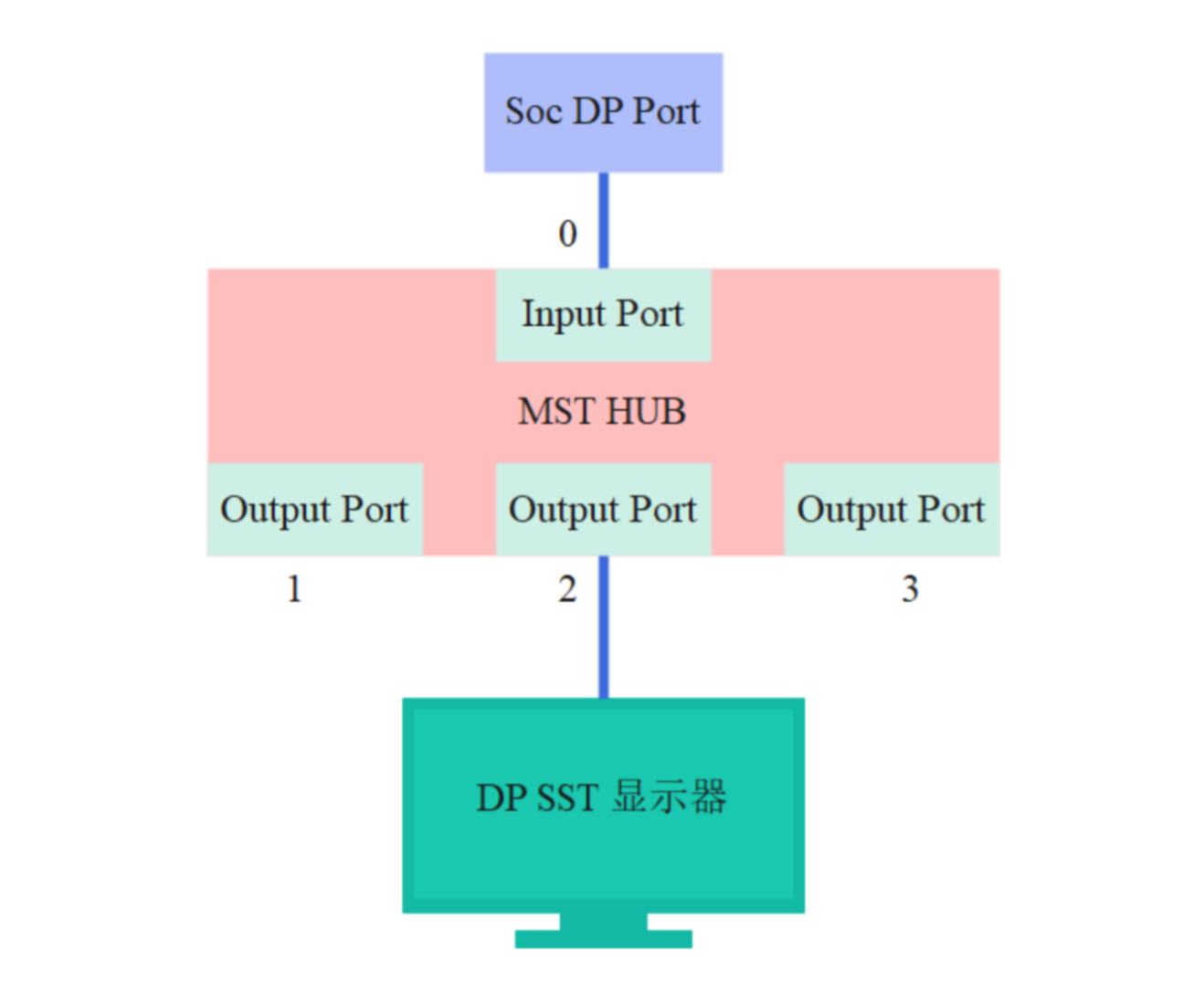
The input and output ports in the above figure are physical interfaces that can be connected to other external devices. According to the DP protocol, the available physical port numbers are 0~7, and the input port number must be smaller than the output port numbers. Generally, MST HUBs start numbering from 0. As shown above, the MST HUB has a total of 4 ports, with Port 0 as the Input Port and Port1/2/3 as Output Ports. Port 2 is connected to an SST display, and the obtained topology information is as follows:
mstb - [00000000c8269fca]: num_ports: 4
       port 3 - [0000000007690f7c] (output - NONE): ddps: 0, ldps: 0, sdp: 0/0, fec: false, conn: 00000000d0584c6f
       port 2 - [00000000812cc57a] (output - SST SINK): ddps: 1, ldps: 0, sdp: 1/1, fec: false, conn: 000000001ef4a070
       port 1 - [00000000efb170aa] (output - NONE): ddps: 0, ldps: 0, sdp: 0/0, fec: false, conn: 000000001455081f
       port 0 - [000000005aa73543] (input - NONE): ddps: 1, ldps: 0, sdp: 0/0, fec: false, conn: 0000000000000000
If an MST monitor is connected, it usually has one DP input and one DP output, as shown below:
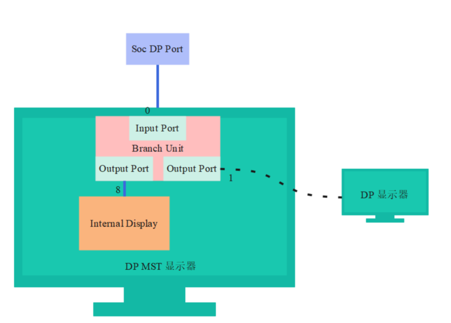 In the above figure, Port0 is the Input Port, Port 1 is the Output port. Port8 is the internal Output port of the monitor. This kind of internal port in MST monitors is a Logical Port, with port numbers from 8 to 15. When the above MST monitor is not daisy-chained with other monitors, the obtained topology information is as follows:
mstb - [0000000019f71241]: num_ports: 3
       port 1 - [0000000095fb1fc0] (output - NONE): ddps: 0, ldps: 0, sdp: 0/0, fec: false, conn: 000000004d03ffa2
       port 8 - [00000000a66da753] (output - SST SINK): ddps: 1, ldps: 0, sdp: 1/2, fec: true, conn: 000000009a417589
       port 0 - [000000009a0122a8] (input - NONE): ddps: 1, ldps: 0, sdp: 0/0, fec: false, conn: 0000000000000000
3.9.2 Atomic state info
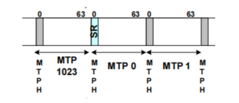
In MST mode, the basic data packet format for DP is called Multi-Stream Transport Packet (MTP). An MTP consists of 64 link symbols, which are also called 64 time slots, numbered from 0 to 63. Time slot 0 is MTPH, and the other time slots can be used to transmit data for each display path. The MTP format is as follows.
 As shown in the payload info table below, port is the port number of the MST device, vcpi is the display path number, slots are the time slots occupied by the corresponding display path, pbn is the bandwidth occupied by the corresponding display path, and sink name is the monitor name.
| idx | port | vcpi | slots | pbn | dsc | sink name |
|---|---|---|---|---|---|---|
| 1 | 1 | 1 | 06-10 | 266 | N | U27U2D |
| 2 | 8 | 2 | 11-15 | 266 | N | DELL U2723QE |
| 3 | 3 | 3 | 01-05 | 266 | N | U28E590 |
3.9.3 DPCD Info
This section is the obtained DPCD information, mainly focusing on the payload table, which records the detailed allocation of time slots.
*** DPCD Info ***
dpcd: 14 1e c4 81 01 11 01 83 2a 3f 04 00 00 00 84
faux/mst: 00 01
mst ctrl: 07
branch oui: 90cc24 devid: SYNAS revision: hw: 1.0 sw: 5.5
payload table: 03 03 03 03 03 03 01 01 01 01 01 02 02 02 02 02 00 00 00 00 00 00
00 00 00 00 00 00 00 00 00 00 00 00 00 00 00 00 00 00 00 00 00 00 00 00 00 00 00
00 00 00 00 00 00 00 00 00 00 00 00 00 00 00
3.9.4 Connector Path Info
connector name is the dynamically registered DP connector, and connector path is the corresponding path.
*** Connector path info ***
connector name | connector path
DP-2             mst:185-1
DP-3             mst:185-2
DP-6             mst:185-3
DP-5             mst:185-2-8
DP-7             mst:185-2-1
4. FAQ
4.1 No Display or Abnormal Display When Inserting DP
First, check if there is the following log:
[   14.857002] rockchip-vop2 fdd90000.vop: [drm:vop2_crtc_atomic_enable] Update mode to 1920x1080p60, type: 10(if:200) for vp2 dclk: 148500000
[   14.857149] rockchip-vop2 fdd90000.vop: [drm:vop2_crtc_atomic_enable] dclk_out2 div: 2 dclk_core2 div: 2
[   14.857868] rockchip-vop2 fdd90000.vop: [drm:vop2_crtc_atomic_enable] set dclk_vop2 to 148500000, get 148500000
[   14.872406] dw-dp fde50000.dp: full-training link: 2 lanes at 5400 MHz
[   14.893269] dw-dp fde50000.dp: clock recovery succeeded
[   14.899797] dw-dp fde50000.dp: channel equalization succeeded
4.1.1 DP Link Training Successful
If the above log appears, it means that the DP connection has been detected and DP has successfully completed link training and is outputting images. The reasons for no display or abnormal display may be as follows:
-
dclk is not divided correctly You can check the following log. The requested dclk is 25.175MHz, but the actual divided clock is 20MHz. If such a clock allocation problem occurs, capture the complete log and provide the clock tree log for further analysis.
 [ 268.733803] rockchip-vop2 fdd90000.vop: [drm:vop2_crtc_atomic_disable] Crtc
 atomic disable vp2
 [ 268.759178] rockchip-vop2 fdd90000.vop: [drm:vop2_crtc_atomic_enable] Update
 mode to 640x480p60, type: 10(if:200) for vp2 dclk: 25175000
 [ 268.759447] rockchip-vop2 fdd90000.vop: [drm:vop2_crtc_atomic_enable] dclk_out2
 div: 2 dclk_core2 div: 2
 [ 268.759665] rockchip_rk3588_pll_set_rate: Invalid rate : 25175000 for pll clk
 pll_v0pll
 [ 268.759715] rockchip-vop2 fdd90000.vop: [drm:vop2_crtc_atomic_enable] set
 dclk_vop2 to 25175000, get 20000000
 [ 268.775591] dw-dp fde50000.dp: full-training link: 4 lanes at 2700 MHz
 [ 268.790059] dw-dp fde50000.dp: clock recovery succeeded
[ 268.795376] dw-dp fde50000.dp: channel equalization succeeded -
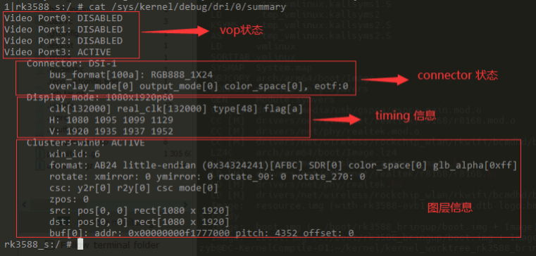
No layer allocated Userspace did not allocate a layer. Execute
cat /sys/kernel/debug/dri/0/summary. If the obtained information is as follows, that is, there is no layer information, further analysis is needed from the userspace part.rk3588_s:/ # cat /sys/kernel/debug/dri/0/summary
Video Port0: DISABLED
Video Port1: DISABLED
Video Port2: DISABLED
Video Port3: ACTIVE
Connector: DSI-1
bus_format[100a]: RGB888_1X24
overlay_mode[0] output_mode[0] color_space[0], eotf:0
Display mode: 1080x1920p60
clk[132000] real_clk[132000] type[48] flag[a]
H: 1080 1095 1099 1129
V: 1920 1935 1937 1952
4.1.2 DP connected
If the log at the beginning of this section does not appear, first check the DP connection status as follows:
cat /sys/class/drm/card0-DP-1/status
If the DP status is connected, first analyze the log for any abnormal errors. If there are errors, analyze from the point of error. If the log is normal, enable the ATOMIC log level for DRM and reproduce the issue to confirm whether there is an abnormal return during drm atomic commit, possibly due to a failure in some step of atomic check.
4.1.3 DP disconnected
For standard DP port output, confirm whether the HPD configuration is correct and whether the hardware connection is normal. For Type-C interfaces, refer to the later section on Type-C interface connection abnormality analysis.
4.2 Type-C Interface Connection Abnormalities
Type-C interface connection abnormalities here refer to issues occurring during the CC and PD phases. First, check the DP connection status:
cat /sys/class/drm/card0-DP-1/status
If there is a connection abnormality, the status obtained here will always be disconnected.
Obtain the tcpm log through the tcpm debug node:
cat /sys/kernel/debug/usb/tcpm-2-0022
A normal connection log is as follows:
[   25.026952] AMS DISCOVER_IDENTITY start
[   25.026967] PD TX, header: 0x176f
[   25.035314] PD TX complete, status: 0
[   25.042866] PD RX, header: 0x524f [1]
[   25.042880] Rx VDM cmd 0xff00a041 type 1 cmd 1 len 5
[   25.042894] AMS DISCOVER_IDENTITY finished
[   25.042898] cc:=4
[   25.052343] Identity: 04e8:a020.0212
[   25.052364] AMS DISCOVER_SVIDS start
[   25.052372] PD TX, header: 0x196f
[   25.061314] PD TX complete, status: 0
[   25.067667] PD RX, header: 0x344f [1]
[   25.067680] Rx VDM cmd 0xff00a042 type 1 cmd 2 len 3
[   25.067695] AMS DISCOVER_SVIDS finished
[   25.067705] cc:=4
[   25.077097] SVID 1: 0xff01
[   25.077114] SVID 2: 0x4e8
[   25.077129] AMS DISCOVER_MODES start
[   25.077135] PD TX, header: 0x1b6f
[   25.086092] PD TX complete, status: 0
[   25.092224] PD RX, header: 0x264f [1]
[   25.092237] Rx VDM cmd 0xff01a043 type 1 cmd 3 len 2
[   25.092252] AMS DISCOVER_MODES finished
[   25.092256] cc:=4
[   25.101432] Alternate mode 0: SVID 0xff01, VDO 1: 0x00000c05
[   25.101517] AMS DISCOVER_MODES start
[   25.101526] PD TX, header: 0x1d6f
[   25.109717] PD TX complete, status: 0
[   25.114919] PD RX, header: 0x284f [1]
[   25.114937] Rx VDM cmd 0x4e8a043 type 1 cmd 3 len 2
[   25.114951] AMS DISCOVER_MODES finished
[   25.114956] cc:=4
[   25.124604] Alternate mode 1: SVID 0x04e8, VDO 1: 0x00000001
[   25.125676] AMS DFP_TO_UFP_ENTER_MODE start
[   25.125686] PD TX, header: 0x1f6f
[   25.134560] PD TX complete, status: 0
[   25.137903] PD RX, header: 0x1a4f [1]
[   25.137917] Rx VDM cmd 0xff01a144 type 1 cmd 4 len 1
[   25.137930] AMS DFP_TO_UFP_ENTER_MODE finished
[   25.137936] cc:=4
[   25.145828] AMS STRUCTURED_VDMS start
[   25.145836] PD TX, header: 0x216f
[   25.154942] PD TX complete, status: 0
[   25.161111] PD RX, header: 0x2c4f [1]
[   25.161125] Rx VDM cmd 0xff01a150 type 1 cmd 16 len 2 //STATUS UPDATE
[   25.161138] AMS STRUCTURED_VDMS finished
[   25.161142] cc:=4
[   25.171888] AMS STRUCTURED_VDMS start
[   25.171911] PD TX, header: 0x236f
[   25.182016] PD TX complete, status: 0
[   25.185550] PD RX, header: 0x1e4f [1]
[   25.185563] Rx VDM cmd 0xff01a151 type 1 cmd 17 len 1 //CONFIGURATION
[   25.185577] AMS STRUCTURED_VDMS finished
[   25.185581] cc:=4
[   26.392673] PD RX, header: 0x204f [1]
[   26.392687] Rx VDM cmd 0xff018106 type 0 cmd 6 len 2 //ATTENTION
From the log, a normal complete process will have DISCOVER_IDENTITY, DISCOVER_MODES, DFP_TO_UFP_ENTER_MODE, STATUS UPDATE, CONFIGURATION, ATTENTION and other command interactions. If the above interaction process does not occur, it means there is an abnormality in the PD interaction.
If the above process is abnormal, you can increase the I2C rate of the PD chip for further testing. If the problem still cannot be solved, you need to provide the complete tcpm log and PD chip log for further analysis.
4.3 AUX_CH Abnormalities
When AUX_CH is abnormal, it will cause abnormal DPCD and EDID read/write operations, and the log may show the following error:
[ 1368.952182] dw-dp fde50000.dp: failed to probe DP link: -110
If you cannot confirm, you can enable the following DRM debug log switch:
echo 0x100 > /sys/module/drm/parameters/debug
Obtain the DPCD read/write log through dmesg. A normal DPCD read/write log is as follows, with ret being 0:
[ 6329.554538] rockchip-drm display-subsystem: [drm:drm_dp_dpcd_probe]
fde50000.dp: 0x00000 AUX -> (ret= 1) 12
[ 6329.554939] rockchip-drm display-subsystem: [drm:drm_dp_dpcd_read]
fde50000.dp: 0x00000 AUX -> (ret= 15) 12 14 c2 81 01 01 01 81 02 02 06 00 00 00
81
[ 6329.555383] rockchip-drm display-subsystem: [drm:drm_dp_dpcd_probe]
fde50000.dp: 0x00000 AUX -> (ret= 1) 12
When AUX_CH is abnormal, the ret value will be an error code, such as:
[   31.116976] rockchip-drm display-subsystem: [drm:drm_dp_dpcd_probe]
fde50000.dp: 0x00000 AUX -> (ret=-110)
Possible causes of AUX_CH abnormalities are as follows.
4.3.1 aux16m clk value abnormal
If the aux16m clk rate is abnormal, the parent clk of aux16m clk is GPLL. By default, GPLL is set to 1188MHz, and the default value of aux16m clk is as follows:
root@RK3588:/# cat /sys/kernel/debug/clk/clk_summary | grep "aux16m"
         clk_aux16m_1               1       2       0   15840000         0
    0 50000
         clk_aux16m_0               1       2       0   15840000         0
    0 50000
If you find that GPLL is not 1188MHz and aux16m clk is also not the default value, please first check whether any modifications have been made to the files in /drivers/clk/rockchip/ based on the SDK, or whether the parent of VOP's DCLK has been reconfigured.
4.3.2 phy power on/off process abnormal
This type of abnormality generally occurs in scenarios where the Type-C interface shares the phy with USB. If one side of the Type-C works normally but switching to the other side causes an error, it may be because the usb phy did not exit when unplugged, resulting in the PHY not being reinitialized when reinserted. You can add logs to confirm whether phy power on/off is executed during USB plug/unplug, and whether the PHY is reinitialized when the other side is reinserted. Log addition can refer to the following patch.
diff --git a/drivers/phy/rockchip/phy-rockchip-usbdp.c
b/drivers/phy/rockchip/phy-rockchip-usbdp.c
index c6fc4a2aa558..6b35e12f40aa 100644
--- a/drivers/phy/rockchip/phy-rockchip-usbdp.c
+++ b/drivers/phy/rockchip/phy-rockchip-usbdp.c
@@ -823,6 +823,7 @@ static int udphy_power_on(struct rockchip_udphy *udphy, u8
mode)
 {
       int ret;
+       dev_info(udphy->dev, "%s status:%x, mode:%x\n", __func__, udphy->status,
mode);
       if (!(udphy->mode & mode)) {
               dev_info(udphy->dev, "mode 0x%02x is not support\n", mode);
               return 0;
@@ -859,6 +860,7 @@ static int udphy_power_off(struct rockchip_udphy *udphy, u8
mode)
 {
       int ret;
+       dev_info(udphy->dev, "%s status:%x, mode:%x\n", __func__, udphy->status,
mode);
       if (!(udphy->mode & mode)) {
               dev_info(udphy->dev, "mode 0x%02x is not support\n", mode);
               return 0;
@@ -883,6 +885,7 @@ static int rockchip_dp_phy_power_on(struct phy *phy)
       struct rockchip_udphy *udphy = phy_get_drvdata(phy);
       int ret, dp_lanes;
+       dev_info(udphy->dev, "%s\n", __func__);
       mutex_lock(&udphy->mutex);
       dp_lanes = udphy_dplane_get(udphy);
@@ -914,6 +917,7 @@ static int rockchip_dp_phy_power_off(struct phy *phy)
       struct rockchip_udphy *udphy = phy_get_drvdata(phy);
       int ret;
+       dev_info(udphy->dev, "%s\n", __func__);
       mutex_lock(&udphy->mutex);
       ret = udphy_dplane_enable(udphy, 0);
       if (ret)
@@ -1028,6 +1032,7 @@ static int rockchip_u3phy_init(struct phy *phy)
       struct rockchip_udphy *udphy = phy_get_drvdata(phy);
       int ret = 0;
+       dev_info(udphy->dev, "%s\n", __func__);
       mutex_lock(&udphy->mutex);
       /* DP only or high-speed, disable U3 port */
       if (!(udphy->mode & UDPHY_MODE_USB) || udphy->hs) {
@@ -1047,6 +1052,7 @@ static int rockchip_u3phy_exit(struct phy *phy)
       struct rockchip_udphy *udphy = phy_get_drvdata(phy);
       int ret = 0;
+       dev_info(udphy->dev, "%s\n", __func__);
       mutex_lock(&udphy->mutex);
       /* DP only or high-speed */
       if (!(udphy->mode & UDPHY_MODE_USB) || udphy->hs)
@@ -1363,6 +1369,7 @@ static int rk3588_udphy_init(struct rockchip_udphy *udphy)
       const struct rockchip_udphy_cfg *cfg = udphy->cfgs;
       int ret;
+       dev_info(udphy->dev, "%s\n", __func__);
       /* enable rx lfps for usb */
       if (udphy->mode & UDPHY_MODE_USB)
               grfreg_write(udphy->udphygrf, &cfg->grfcfg.rx_lfps, true);
4.3.3 DP dual mode adapter cable causes abnormality
DP dual mode requires the DP port to support both DP signal output and HDMI TMDS signal transmission, and the AUX channel to support both DP AUX and DDC (I2C).
RK3588 DP does not support DP dual mode. If a cable supporting DP dual mode is used, it will cause AUX_CH abnormalities. This usually occurs with DP-to-HDMI adapter cables or converters. If you use a DP-to-HDMI adapter cable to connect to an HDMI monitor and encounter AUX_CH abnormalities, and the adapter cable supports HDMI 2.0 or lower protocol versions, it may be because the adapter cable is a DP dual mode cable. It is recommended to replace it with an adapter cable that supports HDMI 2.0 or above.
4.3.4 Signal interference causes abnormality
This problem usually occurs in Type-C direct connection scenarios, where DP AUX is interfered by signals on USB DP/DM. You can confirm by disconnecting USB DP/DM at the hardware level and observing whether the problem recurs. To solve this problem, one way is to use higher quality Type-C cables with proper shielding between signals. Another way is to avoid using USB DP/DM for data transmission.
4.3.5 Hardware abnormality
First, confirm whether the hardware connection path is normal and whether the AUX differential signal is transmitted normally, and check for cold solder joints. Second, check whether the peripheral circuit of the AUX_CH path is designed according to the DP protocol. If a conversion chip is used, first confirm whether the peripheral circuit of the conversion chip is normal.
4.4 4K 120Hz Output Configuration
The default VOP ACLK for RK3588 is 500M. For high pixel clk configurations such as 4K 120Hz output, performance issues may cause the following display abnormalities:
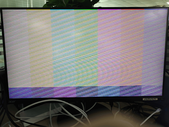
For such problems, the VOP ACLK needs to be increased to 800M:
&vop {
    assigned-clocks = <&cru ACLK_VOP>;
    assigned-clock-rates = <800000000>;
};
Get the VOP ACLK as follows:
cat /sys/kernel/debug/clk/clk_summary | grep "aclk_vop"
4.5 DP Bandwidth Calculation
4.5.1 SST Mode Bandwidth Calculation
Obtain the bandwidth supported by each DP lane, the formula is as follows: $$ bandwidth__per_lane = pixel_clk \times bit_per_pixel \times 1.25 / lane_count $$
Where bit_per_pixel is the number of bits per pixel, 1.25 is the phy lane encoding efficiency, lane_count is the number of available lanes. The final calculation result bandwidth_per_lane is the minimum bandwidth required for each lane. If the current lane rate is less than the required minimum bandwidth, the corresponding pixel clk display mode will be filtered out by the DP driver.
When using adapter cables or docks, you need to confirm whether the lane rate and lane count supported by the adapter cable and dock meet the current bandwidth requirements. If not, you need to replace them with ones that support higher lane rates and more lane counts.
For example, for a dock with 2 lanes and a maximum lane rate of 5.4 Gbps/lane, if you want to output 4K@60Hz with a pixel clock of 594MHz and RGB888 format image data, the required bandwidth per lane is:
$$
bandwidth\_\_per\_lane = 594 \times 24 \times 1.25 / 2 = 8.91\,\text{Gbps/lane} > 5.4\,\text{Gbps/lane}
$$
It can be seen that the current dock does not support outputting 4K@60Hz with a pixel clock of 594MHz and RGB888 format data. You need to use a dock with 4 lane output to increase the PHY lane bandwidth, or output YUV420 format data to reduce the required PHY lane bandwidth.
4.5.2 MST Mode Bandwidth Calculation
The bandwidth calculation in MST mode is similar to that in SST mode. The formula for calculating the bandwidth required for each stream on each lane is the same as in SST mode, but you need to consider whether the total bandwidth will be exceeded when multiple streams are output simultaneously. At the same time, in MST mode, the MTPH header also occupies a certain amount of bandwidth, which needs to be considered as bandwidth loss.
For example, according to the maximum bandwidth supported by RK3576: 4 lanes, 8.1Gbps:
An MTP has 64 time slots, one of which is for MTPH, so the maximum bandwidth supported by each lane is: $$ bandwidth_per_Lane_max=8.1 * 63/64=7.97Gbps $$
For 4096x2160@60Hz, pixel clock 594MHz, RGB888 format display output, the bandwidth occupied by each lane is: $$ bandwidth_per_lane=594 * 24 * 1.25/4=4.46Gbps $$
For 2560x1440@60Hz, pixel clock 297MHz, RGB888 format display output, the bandwidth occupied by each lane is: $$ bandwidth_per_lane=594 * 24 * 1.25/4=2.23Gbps $$
For 1920x1080@60Hz, pixel clock 148.5MHz, RGB888 format display output, the bandwidth occupied by each lane is: $$ bandwidth_per_lane=594 * 24 * 1.25/4=1.12Gbps $$
For RK3576, under the maximum bandwidth of 4 lanes and 8.1Gbps, when three streams are output simultaneously, and the resolutions of the three streams are set as above (4096x2160@60Hz, 2560x1440@60Hz, 1920x1080@60Hz), the total bandwidth consumed per lane is less than the maximum supported bandwidth per lane:
$$ bandwith_per_lane_total = 4.46 + 2.23 + 1.12 = 7.81Gbps < 7.97Gbps < 7.97Gbps $$
This is the maximum capability supported by RK3576 for three simultaneous outputs in MST mode.
4.6 DP Timing Restrictions
For non-standard resolutions, if the porch is too small, DP output may not be possible. Currently, the DP driver limits the minimum HBP to 16 and the minimum HSYNC to 9. If they are below the minimum value, the driver will adjust the corresponding HBP or HSYNC to the supported minimum value.
4.7 MST Mode Usage Restrictions
4.7.1 Capability Limitations
For the DP interface of RK3576, the maximum capability of each output is as follows:
| Stream Channel | Max Width | Max Height | Max Pixel Clock |
|---|---|---|---|
| Stream-0 | 4096 | 2160 | 1188 MHz |
| Stream-1 | 2560 | 1440 | 300 MHz |
| Stream-2 | 1920 | 1080 | 150 MHz |
For the VOP of RK3576, the maximum capability of each Video Port output is as follows:
| VOP Video Port | Max Width | Max Height | Max Pixel Clock |
|---|---|---|---|
| Video Port 0 | 4096 | 2160 | 1200 MHz |
| Video Port 1 | 2560 | 1600 | 300 MHz |
| Video Port 2 | 1920 | 1080 | 150 MHz |
From the output capabilities of VOP and DP, if you want to use DP MST for triple independent display on RK3576 and output the maximum supported resolution, it is recommended to configure Video Port0->DP Stream-0, Video Port1->DP Steam1, Video Port2->DP Stream 2. The DTS configuration is as follows:
&dp0 {
 status = "okay";
};
&dp0_in_vp0 {
 status = "okay";
};
&dp0_in_vp1 {
 status = "disabled";
};
&dp0_in_vp2 {
 status = "disabled";
};
&dp1 {
 status = "okay";
};
&dp1_in_vp0 {
 status = "disabled";
};
&dp1_in_vp1 {
 status = "okay";
};
&dp1_in_vp2 {
 status = "disabled";
};
&dp2 {
 status = "okay";
};
&dp2_in_vp0 {
 status = "disabled";
};
&dp2_in_vp1 {
 status = "disabled";
};
&dp2_in_vp2 {
 status = "okay";
};
If you want to use DP MST for triple mirror display on RK3576, you can only output up to 1920x1080@60Hz. It is recommended to configure Video Port2->DP Stream-0, Video Port2->DP Steam1, Video Port2->DP Stream 2. The DTS configuration is as follows:
&dp0 {
 status = "okay";
};
&dp0_in_vp0 {
 status = "disabled";
};
&dp0_in_vp1 {
 status = "disabled";
};
&dp0_in_vp2 {
 status = "okay";
};
&dp1 {
 status = "okay";
};
&dp1_in_vp0 {
 status = "disabled";
};
&dp1_in_vp1 {
 status = "disabled";
};
&dp1_in_vp2 {
 status = "okay";
};
&dp2 {
 status = "okay";
};
&dp2_in_vp0 {
 status = "disabled";
};
&dp2_in_vp1 {
 status = "disabled";
};
&dp2_in_vp2 {
 status = "okay";
};
4.7.2 Resolution Filtering
In Linux DRM framework, DP MST dynamically registers Connectors, and DP Stream-0/1/2 are registered as 3 Encoders. However, when a Connector is connected, it is not possible to determine which Encoder will be used for output. As in the triple independent display configuration in the previous section, only resolutions not supported by all 3 DP Streams will be filtered, as shown below:
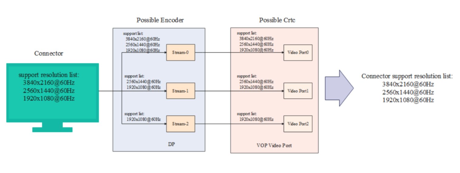
However, due to differences in the output capabilities of each DP Stream and each Vop Video Port, some resolutions may not be output on certain display paths. For example, if you want to output 3840x2160@60Hz on the Video Port2->DP Stream-2 display path, it cannot be displayed normally.
For the above situation, user space applications need to restrict the resolution output for specific display paths. Alternatively, the maximum resolution of the connected display device should not exceed the maximum supported resolution of DP Stream-2.