
DSMC
Chip Name: RK3576
Kernel Version: kernel 6.10
Preface
This document provides instructions and usage methods for kernel development of the ROCKHIP DSMC module.
Target Audience
This document (guide) is mainly intended for the following engineers:
- Technical Support Engineers
- Software Development Engineers
1. Terminology Explanation
- DSMC: Double Data Rate Serial Memory Controller
- PSRAM: Pseudo static random access memory
- DPRAM: Dual Port Random Access Memory
2. Overview
Double Data Rate Serial Memory Controller (DSMC) uses time-division multiplexing of command, address, and data lines, with data transferred on both rising and falling edges, featuring fewer pins and high bandwidth. The data bus width supports x8, x16, and up to 4 chip selects. The transfer protocol supports Hyperbus PSRAM, Xccela PSRAM, and Local bus. If using the Local bus protocol, the slave device must use the RK-developed slave model or a device with the same protocol. If using HYPERBUS PSRAM or XCCELA PSRAM protocols, the slave device supports PSRAM chips from manufacturers such as Winbond, AP memory, Cypress, ISSI, etc.
3. DSMC Driver
3.1 Driver Files
DSMC driver file locations:
drivers/memory/rockchip/dsmc-host.c/* Main driver program */drivers/memory/rockchip/dsmc-controller.c/* DSMC controller behavior configuration */drivers/memory/rockchip/dsmc-lb-device.c/* DSMC Local bus device */
3.2 DTS Node Configuration
dsmc: dsmc@2a280000 {
    ...
    clock-frequency = <100000000>; /* DSMC interface frequency setting */
    ...
    /* Slave device properties */
    slave {
        rockchip,dqs-dll = <0x20 0x20 /* DQS0, DQS1 DLL delay parameters for slave device cs0 */
                           0x20 0x20 /* DQS0, DQS1 DLL delay parameters for slave device cs1 */
                           0x20 0x20 /* DQS0, DQS1 DLL delay parameters for slave device cs2 */
                           0x20 0x20>; /* DQS0, DQS1 DLL delay parameters for slave device cs3 */
        /*
         * rockchip,ranges: Base address and size of DSMC access to slave device memory;
         * If the memory space size of different CS is different, the maximum needs to be configured.
         * rockchip,ranges = <0x0 0x10000000 0x0 0x2000000> means: if the peripheral is PSRAM,
         * each CS is allocated 0x2000000 memory space;
         * if the peripheral is Local Bus, each region is allocated 0x2000000 memory space.
         */
        rockchip,ranges = <0x0 0x10000000 0x0 0x2000000>;
        rockchip,slave-dev = <&dsmc_slave>;
    };
};

dsmc_slave: dsmc_slave {
    compatible = "rockchip,dsmc-slave";
    rockchip,clk-mode = <0>; /* clk mode, only for Local bus */
    status = "disabled";
    /* If the slave device is PSRAM (Hyperbus Psram or Xccela Psram), enable the corresponding cs node */
    psram {
        psram0 {
            status = "disabled"; /* If slave device cs0 is PSRAM, change to "okay" */
        };
        psram1 {
            status = "disabled"; /* If slave device cs1 is PSRAM, change to "okay" */
        };
        psram2 {
            status = "disabled"; /* If slave device cs2 is PSRAM, change to "okay" */
        };
        psram3 {
            status = "disabled"; /* If slave device cs3 is PSRAM, change to "okay" */
        };
    };
    /* If the slave device is a Local bus device, enable and configure the corresponding node */
    lb-slave {
        dsmc_lb_slave0: lb-slave0 {
            status = "disabled"; /* If slave device cs0 is a Local bus device, change to "okay" */
            dsmc_p0_region: region {
                dsmc_p0_region0: region0 { /* Properties of region0 of this slave device */
                    rockchip,attribute = "Merged FIFO";/* region0 is mergeable FIFO of slave device */
                    rockchip,ca-addr-width = <0>; /* CA transfer format, 0: 32bit, 1: 16bit */
                    rockchip,dummy-clk-num = <1>;
                    rockchip,cs0-be-ctrled = <0>; /* slave device cs0 is controlled by cs1,2,3 */
                    rockchip,cs0-ctrl = <0>; /* slave device cs0 controls cs1,2,3 */
                    status = "disabled";
                };
                dsmc_p0_region1: region1 { /* Properties of region1 of this slave device */
                    rockchip,attribute = "No-Merge FIFO";/* region1 is non-mergeable FIFO of slave device */
                    rockchip,ca-addr-width = <0>;
                    rockchip,dummy-clk-num = <1>;
                    rockchip,cs0-be-ctrled = <0>;
                    rockchip,cs0-ctrl = <0>;
                    status = "disabled";
                };
                dsmc_p0_region2: region2 { /* Properties of region2 of this slave device */
                    rockchip,attribute = "DPRA"; /* region2 is DPRAM of slave device */
                    rockchip,ca-addr-width = <0>;
                    rockchip,dummy-clk-num = <1>;
                    rockchip,cs0-be-ctrled = <0>;
                    rockchip,cs0-ctrl = <0>;
                    status = "disabled";
                };
                dsmc_p0_region3: region3 { /* Properties of region3 of this slave device */
                    rockchip,attribute = "Register"; /* region3 is register of slave device */
                    rockchip,ca-addr-width = <0>;
                    rockchip,dummy-clk-num = <1>;
                    rockchip,cs0-be-ctrled = <0>;
                    rockchip,cs0-ctrl = <0>;
                    status = "disabled";
                };
            };
        };
        dsmc_lb_slave1: lb-slave1 {
            status = "disabled"; /* If slave device cs1 is a Local bus device, change to "okay" */
            dsmc_p1_region: region {
                dsmc_p1_region0: region0 {
                    rockchip,attribute = "Merged FIFO";
                    rockchip,ca-addr-width = <0>;
                    rockchip,dummy-clk-num = <1>;
                    rockchip,cs0-be-ctrled = <0>;
                    rockchip,cs0-ctrl = <0>;
                    status = "disabled";
                };
                dsmc_p1_region1: region1 {
                    rockchip,attribute = "No-Merge FIFO";
                    rockchip,ca-addr-width = <0>;
                    rockchip,dummy-clk-num = <1>;
                    rockchip,cs0-be-ctrled = <0>;
                    rockchip,cs0-ctrl = <0>;
                    status = "disabled";
                };
                dsmc_p1_region2: region2 {
                    rockchip,attribute = "DPRA";
                    rockchip,ca-addr-width = <0>;
                    rockchip,dummy-clk-num = <1>;
                    rockchip,cs0-be-ctrled = <0>;
                    rockchip,cs0-ctrl = <0>;
                    status = "disabled";
                };
                dsmc_p1_region3: region3 {
                    rockchip,attribute = "Register";
                    rockchip,ca-addr-width = <0>;
                    rockchip,dummy-clk-num = <1>;
                    rockchip,cs0-be-ctrled = <0>;
                    rockchip,cs0-ctrl = <0>;
                    status = "disabled";
                };
            };
        };
        dsmc_lb_slave2: lb-slave2 {
            status = "disabled"; /* If slave device cs2 is a Local bus device, change to "okay" */
            dsmc_p2_region: region {
                dsmc_p2_region0: region0 {
                    rockchip,attribute = "Merged FIFO";
                    rockchip,ca-addr-width = <0>;
                    rockchip,dummy-clk-num = <1>;
                    rockchip,cs0-be-ctrled = <0>;
                    rockchip,cs0-ctrl = <0>;
                    status = "disabled";
                };
                dsmc_p2_region1: region1 {
                    rockchip,attribute = "No-Merge FIFO";
                    rockchip,ca-addr-width = <0>;
                    rockchip,dummy-clk-num = <1>;
                    rockchip,cs0-be-ctrled = <0>;
                    rockchip,cs0-ctrl = <0>;
                    status = "disabled";
                };
                dsmc_p2_region2: region2 {
                    rockchip,attribute = "DPRA";
                    rockchip,ca-addr-width = <0>;
                    rockchip,dummy-clk-num = <1>;
                    rockchip,cs0-be-ctrled = <0>;
                    rockchip,cs0-ctrl = <0>;
                    status = "disabled";
                };
                dsmc_p2_region3: region3 {
                    rockchip,attribute = "Register";
                    rockchip,ca-addr-width = <0>;
                    rockchip,dummy-clk-num = <1>;
                    rockchip,cs0-be-ctrled = <0>;
                    rockchip,cs0-ctrl = <0>;
                    status = "disabled";
                };
            };
        };
        dsmc_lb_slave3: lb-slave3 {
            status = "disabled"; /* If slave device cs3 is a Local bus device, change to "okay" */
            dsmc_p3_region: region {
                dsmc_p3_region0: region0 {
                    rockchip,attribute = "Merged FIFO";
                    rockchip,ca-addr-width = <0>;
                    rockchip,dummy-clk-num = <1>;
                    rockchip,cs0-be-ctrled = <0>;
                    rockchip,cs0-ctrl = <0>;
                    status = "disabled";
                };
                dsmc_p3_region1: region1 {
                    rockchip,attribute = "No-Merge FIFO";
                    rockchip,ca-addr-width = <0>;
                    rockchip,dummy-clk-num = <1>;
                    rockchip,cs0-be-ctrled = <0>;
                    rockchip,cs0-ctrl = <0>;
                    status = "disabled";
                };
                dsmc_p3_region2: region2 {
                    rockchip,attribute = "DPRA";
                    rockchip,ca-addr-width = <0>;
                    rockchip,dummy-clk-num = <1>;
                    rockchip,cs0-be-ctrled = <0>;
                    rockchip,cs0-ctrl = <0>;
                    status = "disabled";
                };
                dsmc_p3_region3: region3 {
                    rockchip,attribute = "Register";
                    rockchip,ca-addr-width = <0>;
                    rockchip,dummy-clk-num = <1>;
                    rockchip,cs0-be-ctrled = <0>;
                    rockchip,cs0-ctrl = <0>;
                    status = "disabled";
                };
            };
        };
    };
};
Users need to enable the corresponding node according to the actual type of slave device. For PSRAM devices, enable the corresponding psramx node according to the CS number connected on the PCB. The driver will automatically identify whether it is Hyperbus or Xccela Psram. If the slave device is an RK-designed DSMC slave, enable the corresponding lb_slavex node according to the CS number connected on the PCB. In addition, modify the configuration of the corresponding region according to the attributes of the slave device. The clk-mode controls three supported clk behaviors: clk-mode = 0 means no clock when CS is high, clock present when CS is low; clk-mode = 1 means the clock is always present regardless of CS, and the slave can use it as a reference clock, but high frequency operation is not possible and various AC timing adjustable parameters are unavailable; clk-mode = 2 means the clock is present when CS is both high and low, but several clocks will be turned off before and after CS transitions.
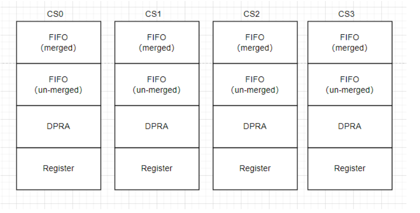
As a Local bus device, the device space diagram is as follows:
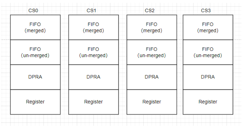
The access space of each slave device chip select CS can be divided into 1, 2, or 4 regions (evenly), just enable the status of the corresponding region property in DTS.
For the rockchip,ranges = <0x0 0x10000000 0x0 0x2000000> property, it configures the start address and size of the slave device memory space, with different meanings for different peripherals.
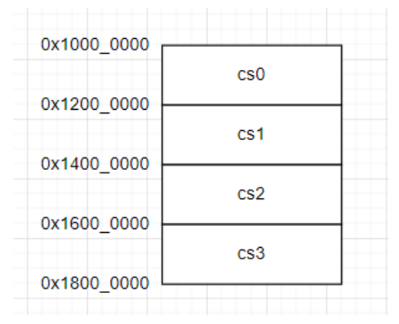
If the peripheral is PSRAM, rockchip,ranges configures the maximum CS space size. The memory space division for each CS is as follows:
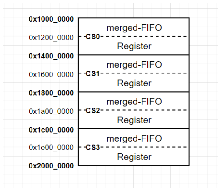
If the peripheral is Local Bus, rockchip,ranges configures the maximum region space size. When only Register and merged-FIFO 2 regions are enabled, the region space division for each CS is as follows:
3.3 Kernel Configuration
Symbol: ROCKCHIP_DSMC [=y]
│
│ Type : bool
│
│ Prompt: Rockchip DSMC(Double Data Rate Serial Memory Controller) driver
│
│ Depends on: MEMORY [=y]
│
│ Location:
│
│ -> Device Drivers
│ -> Memory Controller drivers (MEMORY [=y])
│ -> Rockchip DSMC(Double Data Rate Serial Memory Controller) driver
(ROCKCHIP_DSMC [=y])
4. Kernel Mode Access to DSMC Slave Device Memory
4.1 Calling Driver Interface
In the DSMC driver, drivers/memory/rockchip/dsmc-host.c implements the following access interfaces:
By calling the function rockchip_dsmc_find_device_by_compat() to find the dsmc device and obtain the private parameters of this device. Access to the DSMC slave device by CPU and DMA is implemented through dsmc_dev.ops. Among them, ops->read and ops->write are for CPU read and write access to the DSMC slave device memory space. ops->copy_from is used for DMA to read from the slave device memory and write to the host memory. ops->copy_to is used for DMA to write from the host memory to the slave device memory.
struct rockchip_dsmc_device *rockchip_dsmc_find_dev(void);
static struct dsmc_ops rockchip_dsmc_ops = {
    .read = dsmc_read,
    .write = dsmc_write,
    .copy_from = dsmc_copy_from,
    .copy_from_state = dsmc_copy_from_state,
    .copy_to = dsmc_copy_to,
    .copy_to_state = dsmc_copy_to_state,
};

static void test(void)
{
    u32 cs;
    struct rockchip_dsmc_device *dsmc_dev;
    dsmc_dev = rockchip_dsmc_find_device_by_compat(rockchip_dsmc_get_compat(0));
    if (dsmc_dev == NULL) {
        printk("error: can not find dsmc device\n");
        return 0;
    }
    for (cs = 0; cs < DSMC_MAX_SLAVE_NUM; cs++) {
        if (dsmc_dev->dsmc.cfg.cs_cfg[i].device_type == DSMC_UNKNOWN_DEVICE)
            continue;
        dsmc_dev->ops->write(dsmc_dev, cs, 0, test_addr, test_data);
        /* TODO */
    }
}
4.2 Direct Access
CPU or master can directly access the DSMC slave memory space (supports random address access of Byte, half-word, word; supports cacheable, uncacheable, write combine mapping methods).
5. User Mode Access to DSMC
5.1 Access via Specific Node
When Local bus is enabled, the DSMC driver will create 4 slave device chip selects CS under /dev/dsmc/, and 4 memory regions under each CS, with each attribute corresponding to the DTS description. If you need to access merged-FIFO, it corresponds to region0, and you need to operate the corresponding region node under the corresponding chip select CS. Details are as follows:
- Use the
open()interface to open the corresponding region device node and obtain the file descriptor; - Use the
mmap()system call to map the above region device memory to the process address space and obtain the mapped address; - Read and write device memory;
- Use
munmap()to unmap the memory; - Use
close()to close the file descriptor.
Sample code is as follows:
device_name = "/dev/dsmc/cs0/region0"
wantbytes = 0x200000;
memfd = open(device_name, O_RDWR | O_SYNC);
if (memfd == -1) {
    fprintf(stderr, "failed to open %s for physical memory: %s\n",
            device_name, strerror(errno));
    exit(EXIT_FAILURE);
}
/* Opening the file with the O_SYNC flag and using the MAP_LOCKED flag for mmap operation results in uncached memory space */
buf = (void volatile *) mmap(0, wantbytes, PROT_READ | PROT_WRITE,
                             MAP_SHARED | MAP_LOCKED, memfd,
                             0x0);
if (buf == MAP_FAILED) {
    fprintf(stderr, "failed to mmap %s for physical memory: %s\n",
            device_name, strerror(errno));
    exit(EXIT_FAILURE);
}
bufsize = wantbytes;
halflen = bufsize / 2;
count = halflen / sizeof(u32);
bufa = (u32v *) buf;
bufb = (u32v *) ((size_t) buf + halflen);
test_dsmc(bufa, bufb, count); /* Read and write DSMC slave memory */
if (munmap((void*)buf, wantbytes) == -1) {
    perror("munmap");
    close(memfd);
    exit(EXIT_FAILURE);
}
close(memfd);
5.2 Direct Access
CPU can directly access the DSMC slave memory space mapped by /dev/mem, for example, on RK3576, use the io command to access region0 of DSMC slave memory: io -4 0x10000000.
6. DSMC Slave Memory Space Allocation
The space allocation of DSMC slave is controlled by the rockchip,ranges property, which configures the start address and size of the slave device memory space.
6.1 PSRAM
For example, configure rockchip,ranges = <0x0 0x10000000 0x0 0x2000000>;. If the peripheral is PSRAM, rockchip,ranges configures the maximum CS space size. For the DSMC controller, the capacity of each chip select CS is the same. If different chip select CSs are equipped with PSRAMs of different capacities, users should pay attention to the boundaries when accessing. The memory space division for each CS is as follows:
Note: DSMC theoretically supports different chip select CSs with PSRAMs from different manufacturers and different capacities, but the bus width (x8 or x16) of different chip select CSs must be the same.
6.2 Local bus
If the peripheral is Local Bus, for the DSMC controller, the capacity of each chip select CS is also the same. Each chip select CS can be evenly divided into 1, 2, or 4 regions, and the attribute of each region can be DPRAM, Register, merged FIFO, or un-merged FIFO. If the actual region capacity of each CS is different, users should pay attention to the boundaries when accessing.
For Local Bus, rockchip,ranges configures the maximum region space size.
If a chip select CS enables 2 regions, the size of each region is determined by DTS (the rockchip,ranges = 0x0 0x10000000 0x0 0x2000000 property of the slave device under the DSMC node). The memory space allocation of each region of each CS is as follows:

7. Data Interaction between DSMC Local Bus Host and Slave
7.1 FIFO
When DSMC uses the Local bus protocol and is connected to an RK slave, there is a FIFO on the slave side. When the region attribute accessed is merged-FIFO or un-merged-FIFO, the data transmitted by the host passes through the FIFO and is then written into the slave's memory, such as DDR, SRAM, etc. This FIFO is invisible. For the DSMC host, the DDR or SRAM memory space on the slave side is the slave's memory space. The data written through DSMC will eventually be written into the slave's memory. When using it, pay attention to the management and data consistency of the slave's memory space.
7.2 Register
When DSMC uses the Local bus protocol and is connected to an RK slave, there is a SLAVE_CSR Register. When the region attribute accessed is Register, it is accessing this SLAVE_CSR Register. This can be used for fast information transfer between host and slave.
Registers available for information exchange:
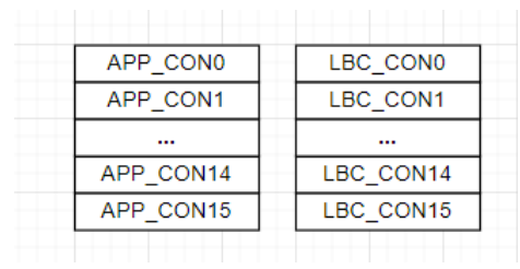
- Among them, the APP_CONx register can be read and written by the slave, and only read by the host;
- The LBC_CONx register can only be read by the slave, and read and written by the host.
When the host writes to the LBC_CONx register, it will trigger a host2slave interrupt to the slave CPU for processing the data sent from the host.
When the slave writes to the APP_CONx register, it triggers a slave2host interrupt through the IO pin INT to the host, and the host CPU can also respond to the interrupt to obtain the data sent by the slave. After DSMC receives the INT signal, it can also initiate a DMA hardware request, and DMA starts to transfer data (DMA needs to be configured in advance).
Typical Scenario 1
The host writes information to the LBC_CONx register, which triggers a host2slave interrupt. The slave reads information from the LBC_CONx register; the slave writes information to the APP_CONx register, which triggers a slave2host interrupt. The host reads information from the APP_CONx register.
Typical Scenario 2:
After the host DSMC and DMA are configured, the host notifies the slave by writing to the LBC_CONx register, then the slave writes to the APP_CONx register, and returns a valid signal to the host from the INT pin. After the DSMC host receives it, it initiates a DMA hardware request to start DMA transfer.
Note:
- APP_CON15 and LBC_CON15 have been used.
- The driver for DSMC using DMA hardware requests has been implemented. When the host DMA configuration is complete, the host writes the original value of LBC_CON15 +1 to the LBC_CON15 register. After the slave receives the data, it writes 1 to APP_CON15 to trigger a slave2host interrupt. After the DSMC host receives it, it automatically initiates a certain number of DMA hardware requests to trigger DMA transfer.