
MIPI DSI2
Chip Name Kernel Version
- RK3576 LINUX Kernel 6.1
- RK3588 LINUX Kernel 5.10/6.1
1. Introduction
DSI-2 is part of a set of communication protocols defined by the MIPI Alliance. DWC-MIPI-DSI2 is a digital core controller that implements all protocol functions defined in the MIPI-DSI2 specification. It is compatible with D-PHY and C-PHY physical interfaces and supports dual Display Stream Compression (DSC) data transmission.
2. MIPI-DSI2 Features
- MIPI® Alliance Specification for Display Serial Interface 2 (DSI-2) Version 1.1
- MIPI® Alliance Specification for Display Command Set (DCS) Version 1.4
- MIPI® Alliance Specification for D-PHY v2.0
- MIPI® Alliance Specification for C-PHY v1.1
- Four data lanes on D-PHY and three data trios on C-PHY
- Bidirectional communication and escape mode through data lane 0
- Continuous and non-continuous clock modes on D-PHY and non-continuous clock mode on C-PHY
- End of Transmission packet (EoTp)
- Scrambling
- VESA DSC 1.1/1.2a
- Up to 4.5 Gbps per lane in D-PHY
- Up to 2.0 Gsps per trio in C-PHY
3. Differences Between RK3576 and RK3588 DSI Interfaces
| Feature | RK3576 | RK3588 |
|---|---|---|
| Dual channel | Not supported | Supported |
| Max resolution | 2560x1600@60Hz | 4096x2304@60Hz |
| Data lanes | 1/2/4 lanes | 1/2/4/8 lanes |
| Max lane rate | D-PHY: 2.5Gbps/lane C-PHY: 1.7Gsps/lane | D-PHY: 4.5Gbps/lane C-PHY: 2.0Gsps/lane |
| Color Format | RGB | RGB |
| Max Color Depth | 10 bit | 10 bit |
| DSC | Not supported | Supported VESA DSC 1.1/1.2a |
| C-PHY | Supported | Supported |
4. Differences Between MIPI DSI-2 Host and MIPI DSI Host
MIPI DSI-2, in addition to being compatible with all protocol functions of MIPI DSI, also adds support for MIPI C-PHY.
5. Differences in MIPI DPHY
The MIPI DPHY on the RK3588 platform differs from previous platform versions, with a maximum bandwidth of up to 4.5 Gbps.

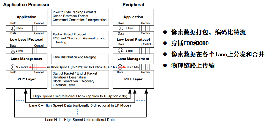
6. Application Areas
MIPI DSI, based on differential signal transmission, can reduce the number of pins and hardware design complexity while maintaining good hardware compatibility. Additionally, MIPI DSI protocol-based IP features low power consumption and low EMI characteristics.
Its application areas are shown in the figure below:
7. Driver Code Description
7.1 uboot
7.1.1 Driver Location
 drivers/video/drm/dw_mipi_dsi2.c
 drivers/video/drm/samsung_mipi_dcphy.c
7.1.2 Driver Configuration
CONFIG_DRM_ROCKCHIP_DW_MIPI_DSI2=y
CONFIG_DRM_ROCKCHIP_SAMSUNG_MIPI_DCPHY=y
7.2 kernel
7.2.1 Driver Location
MIPI DSI-2 host controller:
drivers/gpu/drm/rockchip/dw-mipi-dsi2-rockchip.c
MIPI DCPHY:
drivers/phy/rockchip/phy-rockchip-samsung-dcphy.c
7.2.2 Driver Configuration
CONFIG_ROCKCHIP_DW_MIPI_DSI=y
CONFIG_PHY_ROCKCHIP_SAMSUNG_DCPHY=y
7.2.3 Reference Device Tree
DTS Path:
arch/arm64/boot/dts/rockchip/rk3588-evb.dtsi
arch/arm64/boot/dts/rockchip/rk3588-evb1-lp4.dtsi
arch/arm64/boot/dts/rockchip/rk3588-evb2-lp4.dtsi
arch/arm64/boot/dts/rockchip/rk3588-evb3-lp5.dtsi
arch/arm64/boot/dts/rockchip/rk3588-evb4-lp4.dtsi
arch/arm64/boot/dts/rockchip/rk3588s-evb.dtsi
arch/arm64/boot/dts/rockchip/rk3588s-evb1-lp4x.dtsi
arch/arm64/boot/dts/rockchip/rk3588s-evb2-lp5.dtsi
arch/arm64/boot/dts/rockchip/rk3588s-evb4-lp4x.dtsi
DTS configuration use case scenarios:
rk3588-evb1: dsi0->dphy->1080p_panel && dsi1->dphy->1080p_panel;
rk3588-evb2: dsi1->dphy->1080p_panel;
rk3588-evb3: dsi0->dphy->1080p_panel && dsi1->cphy->cphy_panel;
rk3588-evb4: dsi0->dphy->1080p_panel;
rk3588s-evb1: dsi0->dphy->1080p_panel && dsi1->dphy->cmd_no_dsc_panel;
rk3588s-evb2: dsi0->cphy->cphy_panel & dsi1->dphy->1080p_panel;
rk3588s-evb4: dsi0->dphy->1080p_panel && dsi1->dphy->cmd_dsc_panel;
8. DSI Controller and Panel Configuration
8.1 DTS Configuration
&dsi0 {
    status = "okay";
    //rockchip,lane-rate = <1000>;
    //auto-calculation-mode;
    //disable-hold-mode;
    //support-psr;
};
&dsi0_panel {
    status = "okay";
    compatible = "simple-panel-dsi";
    reg = <0>;
    power-supply = <&vcc3v3_lcd_n>;
    backlight = <&backlight>;
    reset-gpios = <&gpio2 RK_PB4 GPIO_ACTIVE_LOW>;
    reset-delay-ms = <10>;
    enable-delay-ms = <10>;
    prepare-delay-ms = <10>;
    unprepare-delay-ms = <10>;
    disable-delay-ms = <60>;
    dsi,flags = <(MIPI_DSI_MODE_VIDEO | MIPI_DSI_MODE_VIDEO_BURST |
    MIPI_DSI_MODE_LPM | MIPI_DSI_MODE_EOT_PACKET)>;
    dsi,format = <MIPI_DSI_FMT_RGB888>;
    dsi,lanes  = <4>;
    //phy-c-option;
    //compressed-data;
    //slice-width = <720>;
    //slice-height = <65>;
    //version-major = <1>;
    //version-minor = <1>;
    panel-init-sequence = [
    ...
    05 78 01 11
    05 00 01 29
    ];
    panel-exit-sequence = [
    05 00 01 28
    05 00 01 10
    ];
    disp_timings0: display-timings {
        native-mode = <&dsi0_timing0>;
        dsi0_timing0: timing0 {
            clock-frequency = <132000000>;
            hactive = <1080>;
            vactive = <1920>;
            hfront-porch = <15>;
            hsync-len = <4>;
            hback-porch = <30>;
            vfront-porch = <15>;
            vsync-len = <2>;
            vback-porch = <15>;
            hsync-active = <0>;
            vsync-active = <0>;
            de-active = <0>;
            pixelclk-active = <0>;
        };
    };
};
8.2 Configuration Description
8.2.1 General Configuration
| Property | Description | Value |
|---|---|---|
| rockchip,lane-rate | Manually specify MIPI channel rate | Units supported: D-PHY: Mbps/lane or Kbps/lane C-PHY: Msps/lane or Ksps/lane For example, specify 800Mbps: rockchip,lane-rate = <800>;or rockchip,lane-rate = <800000>; |
| auto-calculation-mode | Enable Auto Calculation mode | Boolean string |
| disable-hold-mode | Frame refresh without configuring TE | Boolean string |
| support-psr | Enable PSR function | Boolean string |
| compatible | Compatible string | simple-panel-dsi |
| power-supply | Panel power supply [option] | Relevant regulator reference |
| backlight | Backlight | Backlight reference |
| enable-gpios | Panel enable GPIO [option] | GPIO reference description |
| reset-gpios | Panel reset GPIO | GPIO reference description |
| reset-delay-ms | Panel sequence delay | Refer to panel spec |
| enable-delay-ms | ||
| prepare-delay-ms | ||
| unprepare-delay-ms | ||
| disable-delay-ms | ||
| dsi,flags | DSI2 working mode | cmd mode: MIPI_DSI_MODE_LPM | MIPI_DSI_MODE_EOT_PACKET video mode: MIPI_DSI_MODE_VIDEO | MIPI_DSI_MODE_VIDEO_BURST | MIPI_DSI_MODE_LPM | MIPI_DSI_MODE_EOT_PACKET |
| dsi,format | Pixel data format | MIPI_DSI_FMT_RGB888 MIPI_DSI_FMT_RGB666 MIPI_DSI_FMT_RGB666_PACKED MIPI_DSI_FMT_RGB565 |
| dsi,lanes | MIPI data channels | 1/2/3 trios [cphy] 6 trios [cphy dual channel] 1/2/3/4 lanes [dphy] 8 lanes [dphy dual channel] |
| phy-c-option | C-PHY panel [option] | Boolean string |
| compressed-data | Panel with DSC [option] | Boolean string |
| slice-width | Define DSC slice width [option] | Refer to panel spec |
| slice-height | Define DSC slice height [option] | |
| version-major | Define DSC version [option] | Refer to panel spec |
| version-minor | ||
| panel-init-sequence | Panel power-on initialization sequence | [hex] data_type delay_ms payload_length payload |
| panel-exit-sequence | Panel power-off initialization sequence | |
| display-timing | Panel timing | Refer to panel spec |
8.2.2 Display Timing
8.2.3 dsi,flags
8.2.3.1 CLK Type
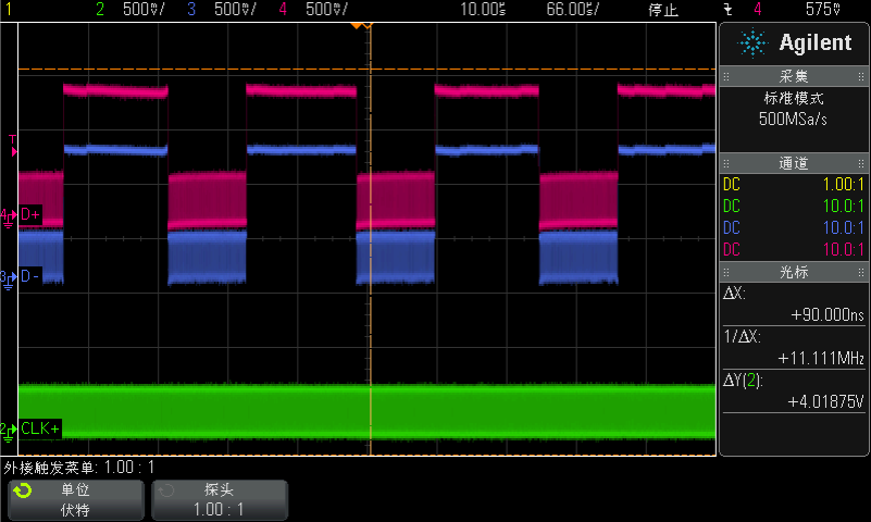
In section 5.6.1 of the MIPI DSI protocol clock requirements, it is introduced that all DSI transmitters and receivers should support continuous clock behavior on the clock channel and may optionally support non-continuous clock behavior. Therefore, whether the clock channel operates in continuous or non-continuous mode in display applications depends on the requirements of the display peripheral.
By default, the clock channel of MIPI DPHY operates in continuous mode, which is the clock behavior supported by both the master and slave in the DSI display system. Additionally, if the DSI peripheral relies on the clock from the host, the clock channel must operate in continuous mode, as shown below:
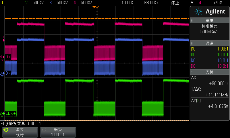
When the system needs to consider power saving, especially during transmission, it can be configured to non-continuous clock mode to avoid wasting power when data transmission is not needed. By adding MIPI_DSI_CLOCK_NON_CONTINUOUS to the dsi,flags, the clock channel of MIPI DPHY will be configured to non-continuous mode, as shown below:
8.2.3.2 Eotp
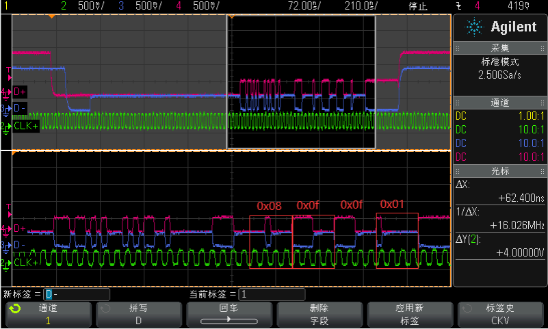
Eotp is not supported in DSI specification version V1.0 and earlier versions. Only devices compliant with newer versions of the DSI specification after V1.0 must support the generation and detection of Eotp. The DSI version of RK3588/RK3576 is V2.0. To ensure interoperability with earlier devices, the host should be able to enable and disable the generation and detection mechanisms. In summary, whether to enable Eotp depends on whether the panel supports it.
Eotp is a short packet used to indicate the end of high-speed transmission on the data link. The main purpose of Eotp is to enhance the robustness of high-speed transmission communication in the system. For this purpose, DSI does not need to send Eotp in LP mode.
Eotp differs from other DSI packets in that it has a fixed format:
- Data Type = DI [5:0] = 0b001000
- Virtual Channel = DI [7:6] = 0b00
- Payload Data [15:0] = 0x0F0F
- ECC [7:0] = 0x01
Adding MIPI_DSI_MODE_EOT_PACKET to the dsi,flags property can enable or disable the transmission of Eotp in high-speed mode by the Soc MIPI DSI TX.
Below is the waveform of Eotp captured in HSDT mode:
8.2.3.3 BLANK_HS_EN
On the data channel, there are generally two LP11 blanks in one line, as shown below:
However, some display modules or external MIPI conversion chips do not support two LP-11s during the Hblank phase. BLK_HFP_HS_EN or BLK_HBP_HS_EN can be added to the dsi,flags property to make HFP or HBP exist in high-speed form.
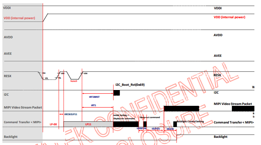
8.2.4 Panel Power-On Timing
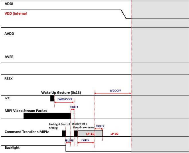
8.2.5 Panel Power-Off Timing
8.2.6 Common Data Types for Initialization Sequence
| Data Type | Description | Packet Size |
|---|---|---|
| 0x03 | Generic Short WRITE, no parameters | Short |
| 0x13 | Generic Short WRITE, 1 parameter | Short |
| 0x23 | Generic Short WRITE, 2 parameters | Short |
| 0x29 | Generic Long WRITE | Long |
| 0x05 | DCS Short WRITE, no parameters | Short |
| 0x15 | DCS Short WRITE, 1 parameter | Short |
| 0x07 | DCS Short WRITE, 1 parameter, DSC EN | Short |
| 0x0a | DCS Long WRITE, PPS, 128 bytes | Long |
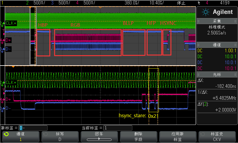
9. Timing for DSI video mode
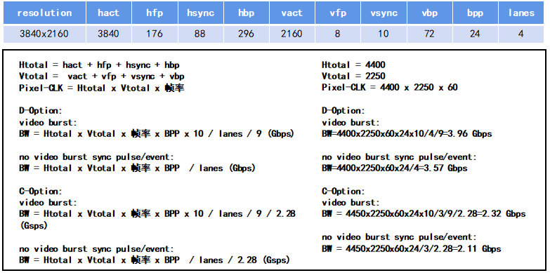
10. Bandwidth
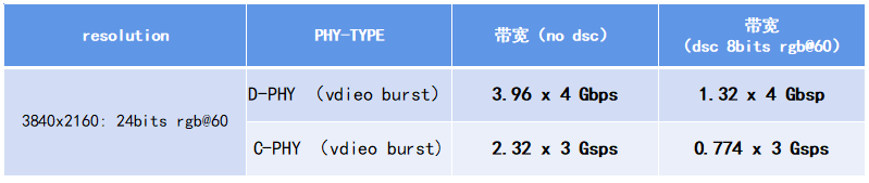
The MIPI DSI driver automatically calculates bandwidth based on the following formulas for different operating modes. During debugging, you may want to fine-tune the calculated results by specifying the rockchip,lane-rate property in the DTS node under the DSI section. The unit can be Kbps/Mbps (D-PHY) or Ksps/Msps (C-PHY). In the bandwidth calculation example below, it can be observed that 4K@60 resolution is fully supported by RK3588 MIPI DSI DPHY without DSC, but CPHY slightly exceeds its maximum bandwidth.
11. DSC
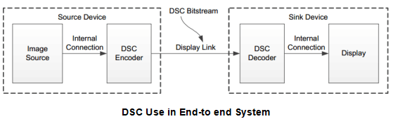
DSC stands for Display Stream Compression. Below is a complete DSC system block diagram. The entire system works in real-time, where uncompressed raw video pixel data is input into the encoder in raster scan order and output as a bitstream. The bitstream is transmitted in real-time through the display link to the decoder, which decodes the received bitstream into the original video pixel data and sends it to the display module for display. The image data format output from the decoder is the same as the input to the encoder. RK3588 has two DSC encoders, which can effectively transmit high-resolution content with low bandwidth and low latency, enabling MIPI DSI to drive higher-resolution displays.
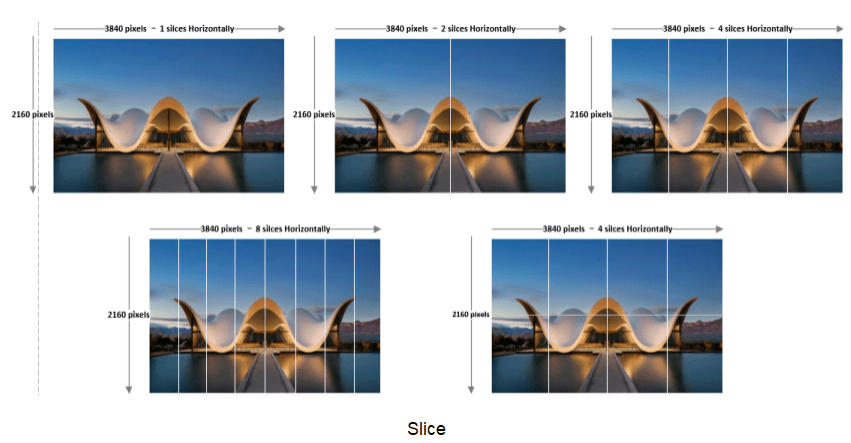
11.1 Slice
To accelerate the encoding process and reduce distortion caused by compression, DSC introduces slices, which divide each frame into sections that are encoded simultaneously. DSC supports 1, 2, 4, 8, or even more slices per line. Note that the unit is slices/line, where a line refers to a row of pixels in raster-scan order. Besides different slice counts, DSC can also use slices of varying widths and heights. For example, in the images below, both have 4 slices per line, but the top-right image uses long, narrow slices, while the bottom-right image uses shorter, rectangular slices. The choice of slice dimensions depends on the DSC capabilities of the source and sink devices and the compression or decompression rate.
RK3588 DSC0 supports up to 8 slices, while DSC1 supports up to 2 slices.
To determine whether RK3588 DSC can support a specific resolution with a certain number of slices, refer to the following formulas:
- DSC_8K:
active_slice_num * slice_width <= 960 * 8 - DSC_4K:
active_slice_num * slice_width <= 2048 * 2
11.2 DSC Encode
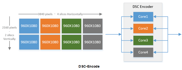
Before compressing image data, the image is evenly divided into slices based on the number of slices supported by both the source and sink devices. For example, in a 3840x2160 resolution, if both devices support 8 slices, the image can be evenly divided into 4 slices horizontally and 2 slices vertically. If the DSC encoder consists of 4 independent cores that process image compression in parallel, the 8 slices on the left side of the image can be divided into 4 groups for simultaneous compression, effectively transmitting 4K content with low bandwidth and low latency.
11.3 DSC Bandwidth
Taking 4Kp60 resolution as an example, the bandwidth of MIPI D/C-PHY before and after enabling DSC changes as follows. After enabling DSC, the link bandwidth can be reduced to one-third to one-half of the original bandwidth.
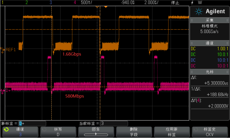
Below is the signal waveform measured when the RK3588 MIPI DSI driver drives a 1440x3120p60 4-lane display module with DSC enabled. The waveforms show the original bandwidth and one-third of the original bandwidth.
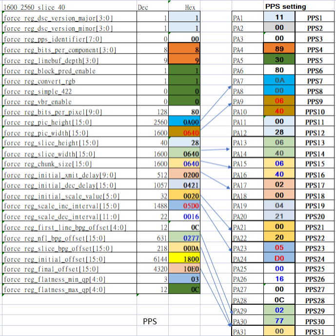
11.4 PPS
PPS (Picture Parameter Set) is 128 bytes long. The table below describes some key information required by the DSC system:
- DSC version;
- Bits per component (BPC) before DSC compression;
- Bits per pixel (BPP) after DSC compression;
- Width and height of the original uncompressed image input to the DSC encoder;
- Width and height of the DSC slice.
11.5 Examples
11.5.1 When to Enable DSC
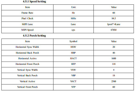
In specific MIPI DSI display solutions, the conditions for enabling DSC can be determined. Below is an example based on the parameters of a display module provided by a customer:
- The module has a DPHY 4 data lanes interface with a maximum rate of 1Gbps/lane;
- The module operates in Video Burst mode, with an original bandwidth of 1.866Gbps for 24-bit RGB at 60fps;
- The module supports DSC with 1 slice;
- The target rate for the module is 676Mbps/lane.
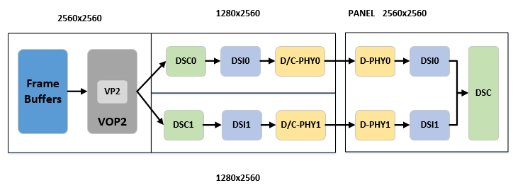
11.5.2 How to Enable DSC for Dual-Channel MIPI
Below is a customer's solution for driving a 2560x2560p120 dual MIPI display module with DSC enabled. The display link diagram is as follows:
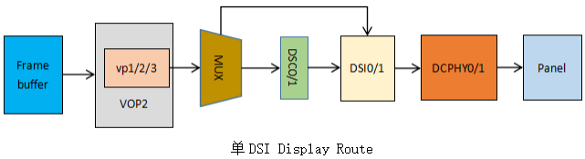
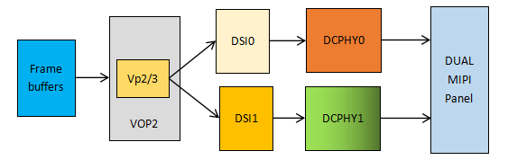
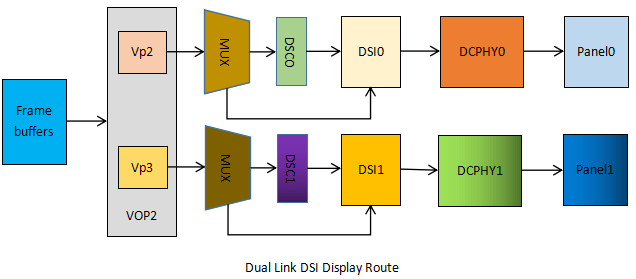
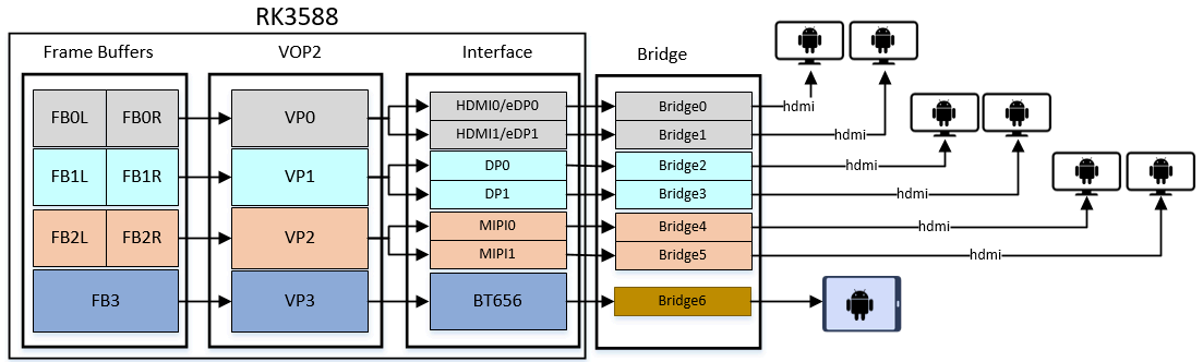
12. Display Route
12.1 MIPI with DSC
12.2 MIPI with DSC Bypass
12.3 DTS Configuration
For example, if DSI0 is mounted on VP3:
&dsi0_in_vp2 {
    status = "disabled";
};
&dsi0_in_vp3 {
    status = "okay";
};
If DSI1 is mounted on VP2:
&dsi1_in_vp2 {
    status = "okay";
};
&dsi1_in_vp3 {
    status = "disabled";
};
13. Boot Logo
13.1 route_dsi0
For example, vp3->dsi0 or vp3->dsc0->dsi0:
&route_dsi0 {
    status = "okay";
    connect = <&vp3_out_dsi0>;
};
13.2 route_dsi1
For example, vp2->dsi1 or vp2->dsc1->dsi1:
&route_dsi1 {
    status = "okay";
    connect = <&vp2_out_dsi1>;
};
13.3 route_dsi0 && route_dsi1
For example, (vp3->dsi0 or vp3->dsc0->dsi0) && (vp2->dsi1 or vp2->dsc1->dsi1):
&route_dsi0 {
    status = "okay";
    connect = <&vp3_out_dsi0>;
};
&route_dsi1 {
    status = "okay";
    connect = <&vp2_out_dsi1>;
};
14. DSI Host
DSI can be configured in Manual or Auto-Calculation mode. By default, the driver is set to Manual mode. Users can choose to configure it in Auto-Calculation mode, which has the following features:
- The host is configured to automatically extract all necessary information and timing parameters from the lPl and PPl interfaces to meet the frame timing requirements in video mode.
- Auto-Calculation mode has the following advantages:
- No need for users to configure a set of registers.
- Simplifies the configuration process and reduces unexpected controller behavior.
- Allows dynamic changes to IPI frames while the controller adapts to output frame changes.
14.1 Single DSI
14.1.1 DSI0
&dsi0 {
    status = "okay";
    //rockchip,lane-rate = <1000>;
    //auto-calculation-mode;
    //disable-hold-mode;
    //support-psr;
    dsi0_panel: panel@0 {
        status = "okay";
        compatible = "simple-panel-dsi";
        ...
        ports {
            #address-cells = <1>;
            #size-cells = <0>;
            port@0 {
                reg = <0>;
                panel_in_dsi: endpoint {
                    remote-endpoint = <&dsi_out_panel>;
                };
            };
        };
    };
    ports {
        #address-cells = <1>;
        #size-cells = <0>;
        port@1 {
            reg = <1>;
            dsi_out_panel: endpoint {
                remote-endpoint = <&panel_in_dsi>;
            };
        };
    };
};
&mipi_dcphy0 {
    status = "okay";
};
14.1.2 DSI1
&dsi1 {
    status = "okay";
    //rockchip,lane-rate = <1000>;
    //auto-calculation-mode;
    //disable-hold-mode;
    //support-psr;
    dsi1_panel: panel@0 {
        status = "okay";
        compatible = "simple-panel-dsi";
        ...
        ports {
            #address-cells = <1>;
            #size-cells = <0>;
            port@0 {
                reg = <0>;
                panel_in_dsi1: endpoint {
                    remote-endpoint = <&dsi1_out_panel>;
                };
            };
        };
    };
    ports {
        #address-cells = <1>;
        #size-cells = <0>;
        port@1 {
            reg = <1>;
            dsi1_out_panel: endpoint {
                remote-endpoint = <&panel_in_dsi1>;
            };
        };
    };
};
&mipi_dcphy1 {
    status = "okay";
};
14.2 Dual-Channel DSI
MODE1:
MODE2:

For dual-channel configuration, note the following highlighted properties:
rockchip,dual-channel = <&dsi1>;
dsi,lanes = <8>; // For DPHY screens, change to 6 for CPHY screens.
&dsi0 {
    status = "okay";
    rockchip,dual-channel = <&dsi1>;
    //auto-calculation-mode;
    //disable-hold-mode;
    //support-psr;
    dsi0_panel {
        status = "okay";
        compatible = "simple-panel-dsi";
        dsi,lanes = <8>;
        ...
        display-timings {
            native-mode = <&timing0>;
            timing0: timing0 {
                clock-frequency = <260000000>;
                hactive = <1440>;
                vactive = <2560>;
                hfront-porch = <150>;
                hsync-len = <30>;
                hback-porch = <60>;
                vfront-porch = <8>;
                vsync-len = <4>;
                vback-porch = <4>;
                hsync-active = <0>;
                vsync-active = <0>;
                de-active = <0>;
                pixelclk-active = <0>;
            };
        };
        ports {
            #address-cells = <1>;
            #size-cells = <0>;
            port@0 {
                reg = <0>;
                panel_in_dsi0: endpoint {
                    remote-endpoint = <&dsi0_out_panel>;
                };
            };
        };
    };
    ports {
        #address-cells = <1>;
        #size-cells = <0>;
        port@1 {
            reg = <1>;
            dsi0_out_panel: endpoint {
                remote-endpoint = <&panel_in_dsi0>;
            };
        };
    };
};
&dsi1 {
    status = "okay";
};
&mipi_dcphy0 {
    status = "okay";
};
&mipi_dcphy1 {
    status = "okay";
};
14.3 Dual-link DSI
&dsi0 {
    status = "okay";
    //rockchip,lane-rate = <1000>;
    //auto-calculation-mode;
    //disable-hold-mode;
    //support-psr;
    dsi0_panel: panel@0 {
        status = "okay";
        compatible = "simple-panel-dsi";
        ...
        ports {
            #address-cells = <1>;
            #size-cells = <0>;
            port@0 {
                reg = <0>;
                panel_in_dsi: endpoint {
                    remote-endpoint = <&dsi_out_panel>;
                };
            };
        };
    };
    ports {
        #address-cells = <1>;
        #size-cells = <0>;
        port@1 {
            reg = <1>;
            dsi_out_panel: endpoint {
                remote-endpoint = <&panel_in_dsi>;
            };
        };
    };
};
&dsi1 {
    status = "okay";
    //rockchip,lane-rate = <1000>;
    //auto-calculation-mode;
    //disable-hold-mode;
    //support-psr;
    dsi1_panel: panel@0 {
        status = "okay";
        compatible = "simple-panel-dsi";
        ...
        ports {
            #address-cells = <1>;
            #size-cells = <0>;
            port@0 {
                reg = <0>;
                panel_in_dsi1: endpoint {
                    remote-endpoint = <&dsi1_out_panel>;
                };
            };
        };
    };
    ports {
        #address-cells = <1>;
        #size-cells = <0>;
        port@1 {
            reg = <1>;
            dsi1_out_panel: endpoint {
                remote-endpoint = <&panel_in_dsi1>;
            };
        };
    };
};
&mipi_dcphy0 {
    status = "okay";
};
&mipi_dcphy1 {
    status = "okay";
};
14.4 DSI Application Scenarios
14.4.1 DSI + SerDer Solution
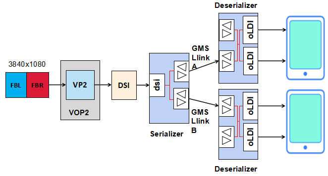
14.4.2 Multi-Screen Connection Solution
15. DC-PHY
In actual application configurations, it is usually set to D-PHY. As can be seen from the display end configuration introduction, it can be configured to C-PHY in the following way:
dsi0_panel: panel@0 {
    ...
    phy-c-option;
    ...
};
15.1 D-PHY
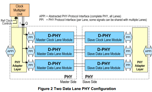
- Up to 4.5 Gbps per lane in D-PHY;
- A D-PHY port can have up to 4 lanes, each lane consists of two differential lines;
- D stands for the Roman numeral 500 or "D". When D-PHY was first introduced, the maximum data rate was 1G (DDR), and the corresponding clock rate was 500MHz. Now the D-PHY rate is no longer limited to these, so the meaning of "D" is no longer relevant.
15.2 C-PHY
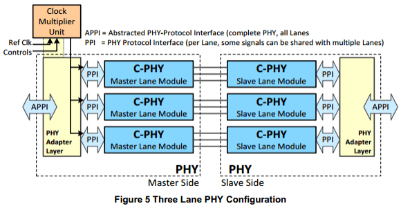
- Up to 2.0 Gsps per trio in C-PHY;
- A C-PHY port can have up to 3 lanes, each lane consists of tree-wire-trios;
- C-PHY does not have a separate clock channel, its clock is embedded in the communication timing;
- C stands for Channel-limited, the channel is limited to 3, C-PHY has a total of 3 lanes, each lane uses 3-wire transmission mode.
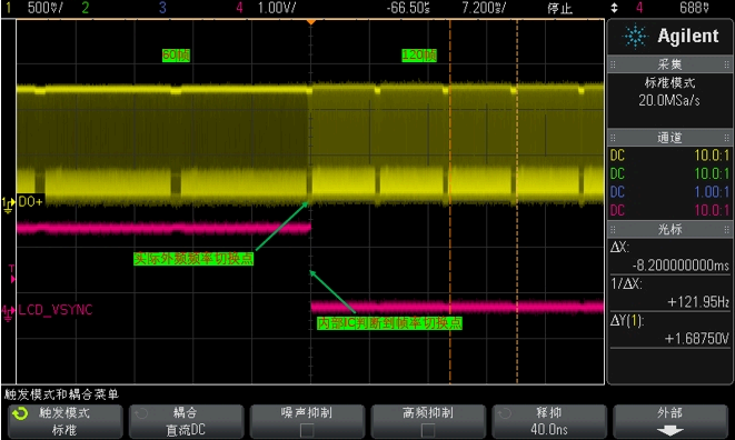
16. Dynamic Frame Rate
MIPI DSI can achieve dynamic frame rate switching, such as between 120fps <-> 60fps, for more details refer to the related document 《Rockchip_RK3588_Developer_Guide_Vsync_Adjust_CN》.
17. PSR
When MIPI DSI works in COMMAND mode, the display panel has a built-in GRAM. It can choose to turn off the DSI output of the main control to reduce power consumption while the display system refreshes static frames. The display panel continues to refresh static frames from the GRAM, and when there is any change in the display content of the new frame, the main control side must enable and refresh the frame in the GRAM of the screen to update the display.
18. Protocol Analysis
18.1 DSI Layer Definitions
18.2 D Option
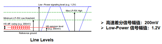
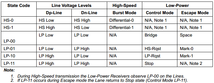
18.2.1 Lane states and line levels
The table below lists all possible channel states that may occur during the normal operation of the DPHY Lane.
18.2.2 Global Operation Flow Diagram
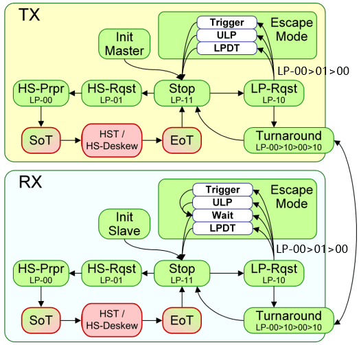
The DSI data channel can be driven to the following three modes:
- Escape Mode (only Dp0/Dn0 will operate in this mode);
- Bus Turnaround Request (only Dp0/Dn0 will operate in this mode);
- High-Speed Data Transmission。
These three modes and the sequence to enter the corresponding mode are defined as follows:
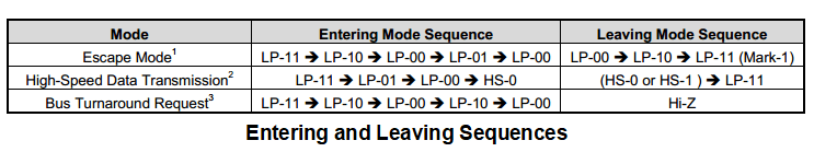
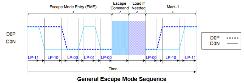
18.2.2.1 Escape Modes
When the data channel is in LP mode, data channel 0 is used for Escape Mode. The data channel should enter Escape Mode through the sequence LP-11->LP-10->LP-00->LP 01->LP-00, and exit Escape Mode through LP-00->LP-10->LP-11.
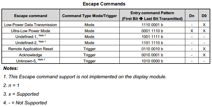
18.2.2.1.1 Escape Commands
Once the data channel enters Escape mode, the transmitter should send 8-bit Escape Commands to indicate the requested behavior. The Escape Commands are as follows:
18.2.2.1.2 LPDT
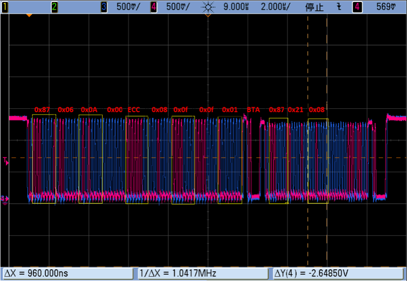
When the data channel enters Escape mode and sends the Low-Power Data Transmission (LPDT) sequence to the display module, the MIPI DSI TX of the Soc can send data to the display module in LPDT mode, which is generally the way to download the initialization sequence to the MIPI display module.
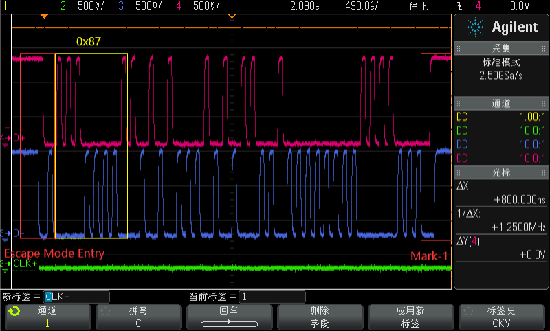
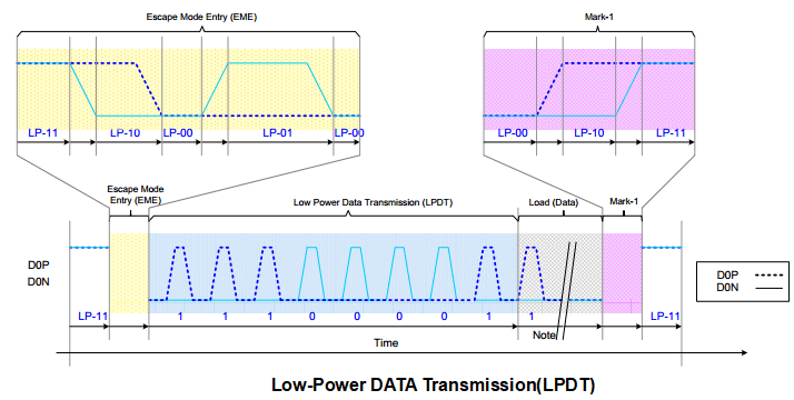 The waveform captured by the oscilloscope in LPDT is as follows:
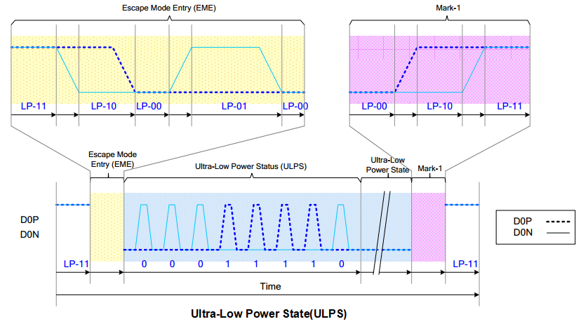
18.2.2.1.3 ULPS
18.2.2.2 HSDT
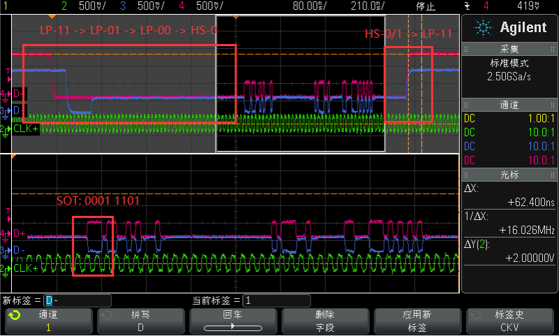
When the clock channel of DPHY is in high-speed clock mode, the display module can enter high-speed data transmission mode, all data channels simultaneously enter high-speed data transmission mode, but may not exit high-speed mode at the same time. The data channel enters high speed mode through the following sequence:
- Start: LP-11
- HS-Request: LP-01
- HS-Settle: LP-00 -> HS-0 (RX: Lane Termination Enable)
- Rx Synchronization: SoT(0001_1101)
- End: High-Speed Data Transmission (HSDT) - Ready to receive High-Speed Data Load
The process of exiting high-speed data transmission mode: Immediately switch the differential state bit after the last有效负载数据 and maintain this state for a period of time Ths-trail.
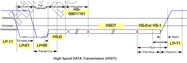
The waveform captured by the oscilloscope in HSDT is as follows:
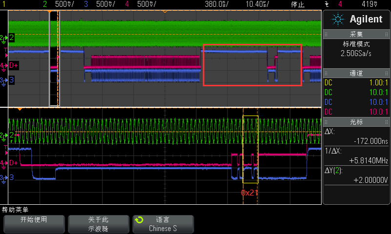
18.2.2.3 BTA
When information needs to be obtained from the display module, the first data channel of Soc DPHY can execute the bus turnaround steps. The operation steps are as follows:
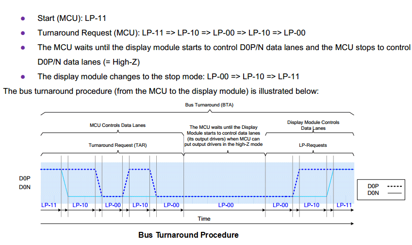
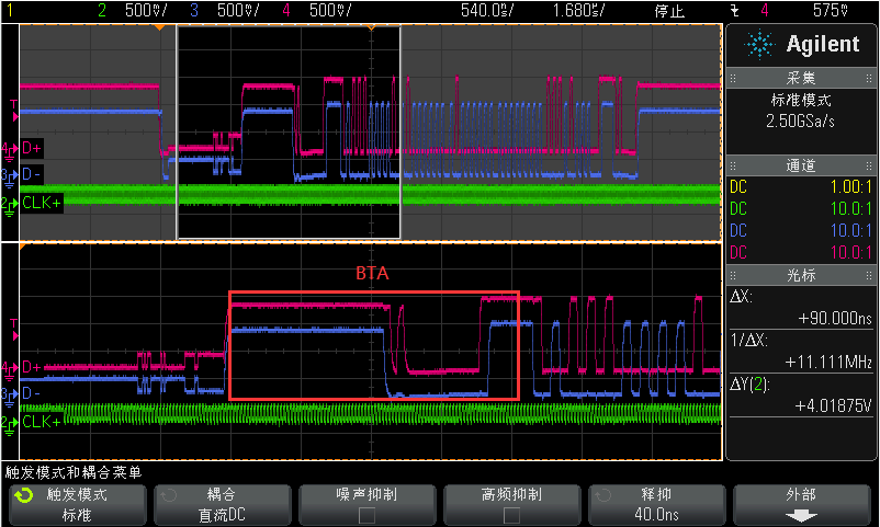
The BTA waveform captured by the oscilloscope when reading back from the display module in HSDT is as follows:
18.2.3 Endian Policy
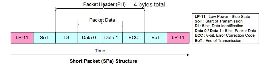
Whether in LP or HS data transmission mode, the data is packed and transmitted to the display module in the form of long packets and short packets.
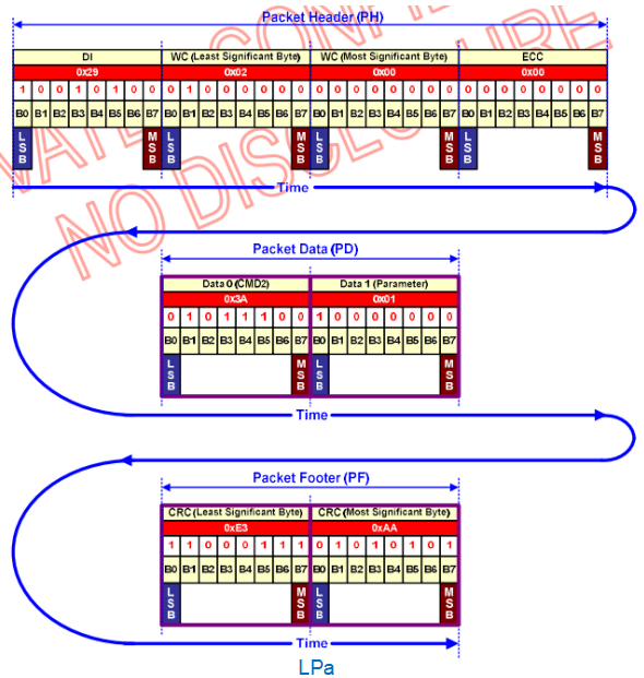
18.2.3.1 SPa
Example:
18.2.3.1.1 LPDT-SPa
The SPa waveform sent to the display module in LPDT and captured by the oscilloscope is as follows:
18.2.3.1.2 HSDT-SPa
The SPa waveform sent to the display module in HSDT and captured by the oscilloscope is as follows:
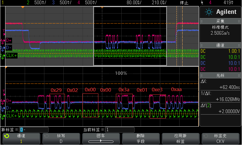
18.2.3.2 LPa
 Example:
18.2.3.2.1 LPDT-LPa
The LPa waveform sent to the display module in LPDT and captured by the oscilloscope is as follows:
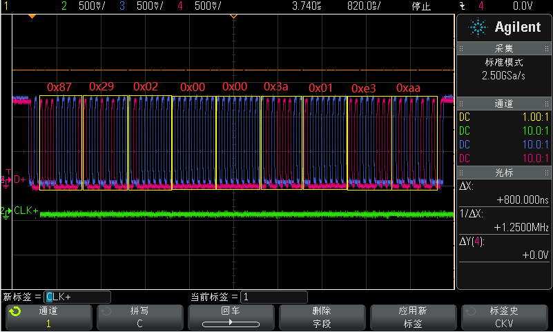
18.2.3.2.2 HSDT-LPa
The LPa waveform sent to the display module in HSDT and captured by the oscilloscope is as follows:
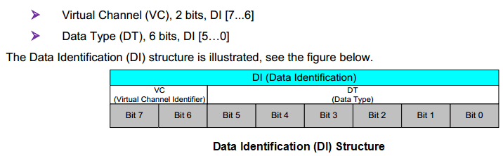
18.2.3.3 DI
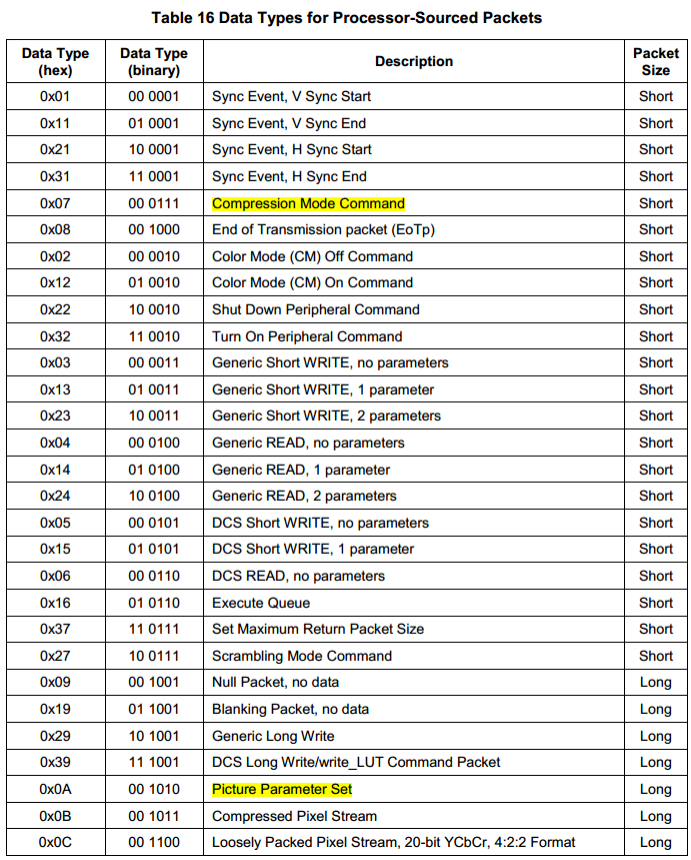
As mentioned above, both SPa and LPa have a Data Identification (DI). Whether a packet is a long or short packet is determined by the DI, which is part of the packet header and consists of two parts:
Most of the data types currently defined in the MIPI protocol are as follows:
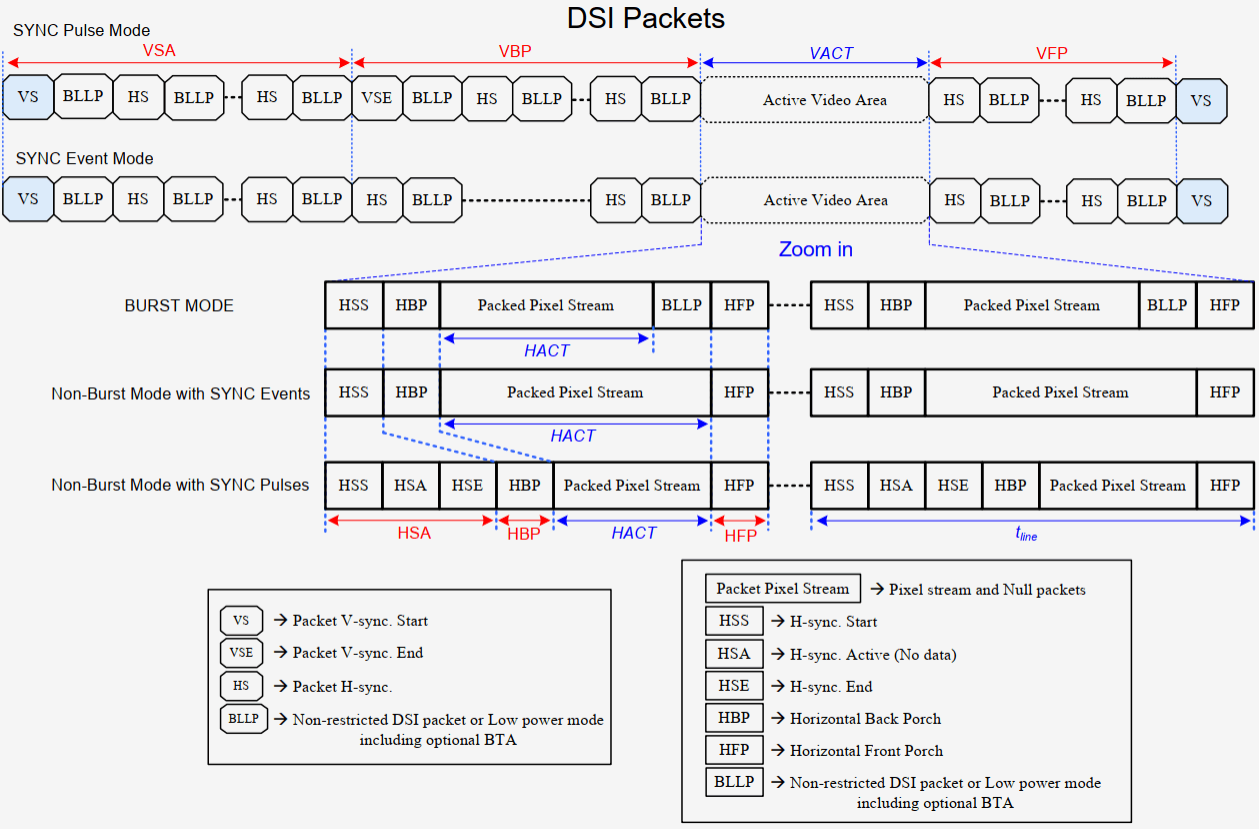
18.2.4 Video Mode Interface Timing
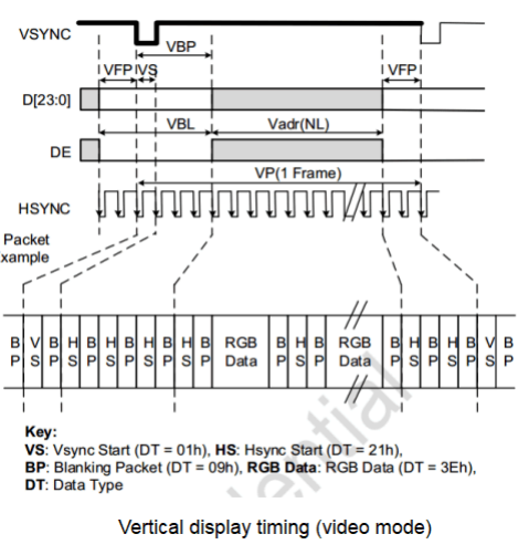
18.2.4.1 Vertical Display Timing (Video mode)
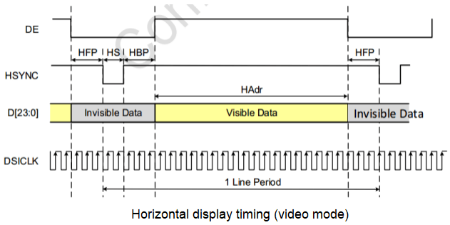
18.2.4.2 Horizontal Display Timing (Video mode)
18.2.4.3 Non-Burst Mode with Sync Pulses
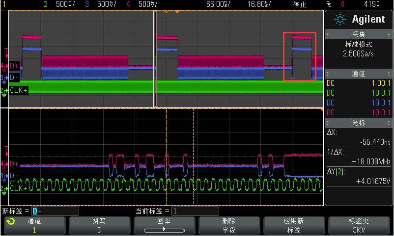
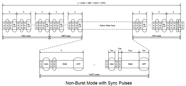 The waveform captured by the oscilloscope for Non-Burst Sync Pulse is as follows:
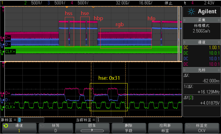
18.2.4.4 Burst Mode
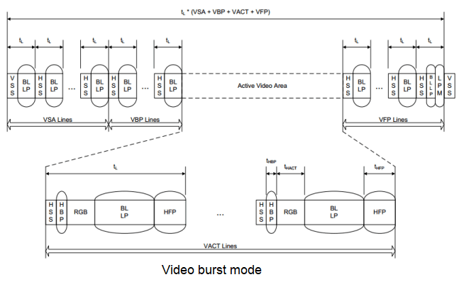 The waveform captured by the oscilloscope for Video Burst is as follows:
19. Common Issues
19.1 View VOP timing and Connector Information
console:/ # cat /d/dri/0/summary
Video Port0: DISABLED
Video Port1: DISABLED
Video Port2: DISABLED
Video Port3: ACTIVE
 Connector: DSI-2
 bus_format[100a]: RGB888_1X24
 overlay_mode[0] output_mode[0] color_space[0]
 Display mode: 1080x1920p60
 clk[132000] real_clk[132000] type[48] flag[a]
 H: 1080 1095 1099 1129
 V: 1920 1935 1937 1952
Cluster3-win0: ACTIVE
 win_id: 6
 format: AB24 little-endian (0x34324241) SDR[0] color_space[0]
 glb_alpha[0xff]
 rotate: xmirror: 0 ymirror: 0 rotate_90: 0 rotate_270: 0
 csc: y2r[0] r2y[0] csc mode[0]
 zpos: 0
 src: pos[0, 0] rect[1080 x 1920]
 dst: pos[0, 0] rect[1080 x 1920]
 buf[0]: addr: 0x000000000376e000 pitch: 4352 offset: 0
19.2 View DSI2 Related Clock Tree
When MIPI works in non-DSC mode, the rate of the MIPI interface is 4 pixels per clock cycle, and the related clocks should meet the following relationship:
video_timing_pixel_rate / 4 = mipi_pixel_clock × K = dclk_out × K = dclk_core
When MIPI works in DSC mode, the related clocks should meet the following relationship:
mipi_pixel_clock = cds_clk / 2
Note! By default, K = 1, when MIPI is configured as dual-channel display mode, K = 2.
console:/ # cat /d/clk/clk_summary | grep vop
   clk_vop_pmu                   0    0    0    24000000    0   0  50000
         dclk_vop3               1    2    0    33000000    0   0  50000
         dclk_vop1_src           0    1    0   594000000    0   0  50000
             dclk_vop1            0    1    0   594000000    0   0  50000
         dclk_vop0_src           0    1    0   594000000    0   0  50000
             dclk_vop0            0    1    0   594000000    0   0  50000
             aclk_vop_low_root    1    1    0   396000000    0   0  50000
             hclk_vop_root        2    4    0   198000000    0   0  50000
               hclk_vop          1    3    0   198000000    0   0  50000
         aclk_vop_root           1    1    0   500000000    0   0  50000
             aclk_vop_doby        0    0    0   500000000    0   0  50000
             aclk_vop_sub_src     1    1    0   500000000    0   0  50000
               aclk_vop          1    4    0   500000000    0   0  50000
             pclk_vop_root        3    5    0   100000000    0   0  50000
         dclk_vop2_src           1    1    0   148500000    0   0  50000
             dclk_vop2            1    2    0   148500000    0   0  50000
console:/ # cat /d/clk/clk_summary | grep dsi
               pclk_dsihost1     1    2    0   100000000    0   0  50000
               pclk_dsihost0     1    2    0   100000000    0   0  50000
   clk_dsihost1                  1    2    0   351000000    0   0  50000
   clk_dsihost0                  1    2    0   351000000    0   0  50000
console:/ # cat /d/clk/clk_summary | grep mipi
         mipi1_clk_src           0    0    0    33000000    0    0  50000
             mipi1_pixclk         0    0    0    33000000    0    0  50000
         mipi0_clk_src           0    0    0   148500000    0    0  50000
             mipi0_pixclk         0    0    0   148500000    0    0  50000
   clk_usbdpphy_mipidcpphy_ref   5    5    0    24000000    0    0  50000
   clk_mipi_camaraout_m4         0    0    0    24000000    0    0  50000
   clk_mipi_camaraout_m3         0    0    0    24000000    0    0  50000
   clk_mipi_camaraout_m2         0    0    0    24000000    0    0  50000
   clk_mipi_camaraout_m0         0    0    0    24000000    0    0  50000
         clk_mipi_camaraout_m1   0    0    0    37125000    0    0  50000
               pclk_mipi_dcphy1  1    1    0   100000000    0    0  50000
               pclk_mipi_dcphy0  1    1    0   100000000    0    0  50000
console:/ #
19.3 How to View the Specified DSI Lane Rate
There are two ways to specify the DSI lane rate, one is automatic calculation by the driver
dmesg | grep dsi
[   77.369812] dw-mipi-dsi2 fde20000.dsi: [drm:dw_mipi_dsi2_encoder_enable] final
DSI-Link bandwidth: 879 x 4 Mbps
The other is manually specified by the following property:
&dsi0 {
 ...
 rockchip,lane-rate = <1000>;
 ...
}
19.4 MIPI DSI2 HOST does not have its own color bar function, you can use the following commands to let VOP2 display the color bar
Select the corresponding command according to the display route:
19.4.1 RK3588
vp0:
io -4 0xfdd90c08 0x1 && io -4 0xfdd90000 0xffffffff
vp1:
io -4 0xfdd90d08 0x1 && io -4 0xfdd90000 0xffffffff
vp2:
io -4 0xfdd90e08 0x1 && io -4 0xfdd90000 0xffffffff
vp3:
io -4 0xfdd90f08 0x1 && io -4 0xfdd90000 0xffffffff
19.4.2 RK3576
vp0:
io -4 0x27d00c08 0x1 && io -4 0x27d00000 0xffffffff
vp1:
io -4 0x27d00d08 0x1 && io -4 0x27d00000 0xffffffff
vp2:
io -4 0x27d00e08 0x1 && io -4 0x27d00000 0xffffffff
19.5 How to Determine Whether MIPI DSI2 and Panel are Communicating Normally When Display Abnormalities Occur
U-Boot
--- a/drivers/video/drm/rockchip_panel.c
+++ b/drivers/video/drm/rockchip_panel.c
@@ -260,6 +260,7 @@ static void panel_simple_prepare(struct rockchip_panel
*panel)
 struct rockchip_panel_priv *priv = dev_get_priv(panel->dev);
 struct mipi_dsi_device *dsi = dev_get_parent_platdata(panel->dev);
 int ret;
+ u8 mode;
 if (priv->prepared)
 return;
@@ -285,6 +286,8 @@ static void panel_simple_prepare(struct rockchip_panel
*panel)
 if (plat->delay.init)
 mdelay(plat->delay.init);
+ mipi_dsi_dcs_get_power_mode(dsi, &mode);
+ printf("===>mode: 0x%x\n", mode);
 if (plat->on_cmds) {
 if (priv->cmd_type == CMD_TYPE_SPI)
 ret = rockchip_panel_send_spi_cmds(panel->state,
@@ -298,6 +301,8 @@ static void panel_simple_prepare(struct rockchip_panel
*panel)
 printf("failed to send on cmds: %d\n", ret);
 }
+ mipi_dsi_dcs_get_power_mode(dsi, &mode);
+ printf("===>mode: 0x%x\n", mode);
 priv->prepared = true;
 }
Kernel
--- a/drivers/gpu/drm/panel/panel-simple.c
+++ b/drivers/gpu/drm/panel/panel-simple.c
@@ -506,6 +506,7 @@ static int panel_simple_prepare(struct drm_panel *panel)
 unsigned int delay;
 int err;
 int hpd_asserted;
+ u8 mode;
 if (p->prepared)
 return 0;
@@ -554,6 +555,8 @@ static int panel_simple_prepare(struct drm_panel *panel)
 }
 }
+ mipi_dsi_dcs_get_power_mode(p->dsi, &mode);
+ printk("===>mode: 0x%x\n", mode);
 if (p->desc->init_seq)
 if (p->dsi)
 panel_simple_xfer_dsi_cmd_seq(p, p->desc->init_seq);
@@ -561,6 +564,9 @@ static int panel_simple_prepare(struct drm_panel *panel)
 if (p->desc->delay.init)
 msleep(p->desc->delay.init);
+ mipi_dsi_dcs_get_power_mode(p->dsi, &mode);
+ printk("===>mode: 0x%x\n", mode);
+
 p->prepared = true;
 return 0;
Normal communication will have the following print, otherwise check the screen end timing to ensure the screen is ready:
===> mode: 0x8
===> mode: 0x9c
19.5.1 get_power_mode Two Types of Readback Waveforms
19.5.1.1 Screen End Normally Returns 0x08 (0x11, 0x29 Not Issued) Waveform as Follows
19.5.1.2 Screen End Normally Returns 0x9c (0x11, 0x29 Issued) Waveform as Follows
19.6 drm Driver Not Bound
Use the following command to check if there is an abnormal binding of a component, for example, if the DP PHY is not enabled, it will cause DP binding exception:
/sys/kernel/debug/device_component/display-subsystem <
master name status
-------------------------------------------------------------
display-subsystem bound
device name � status
-------------------------------------------------------------
fdd90000.vop bound
fde20000.dsi bound
fde30000.dsi bound
fde50000.dp bound
19.7 backlight Driver Probe Failed
console:/ # dmesg | grep backlight
[    3.164274] pwm-backlight: probe of backlight failed with error -16
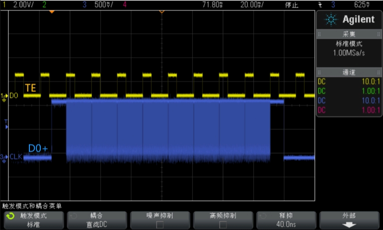
19.8 Command Mode Display Module How to Configure TE
To prevent image tearing, the refresh rate of the display controller should be consistent with the refresh rate of the display module from the GRAM. RK3588 and RK3576 only support the method of externally feeding back the TE signal from the display module.
19.8.1 Hardware TE
MIPI DSI has dedicated PINs that can be reused as te.
&dsi0 {
 ...
 /* TE signal of the display module is connected to MIPI_TE0 */
 pinctrl-names = "default";
 pinctrl-0 = <&mipi_te0>;
 ...
};
&dsi1 {
 ...
 /* TE signal of the display module is connected to MIPI_TE1, only RK3588 support dsi1 */
 pinctrl-names = "default";
 pinctrl-0 = <&mipi_te1>;
 ...
};
19.8.2 Software TE
Sometimes the hardware TE may be reused for other functions, so other unused GPIOs can be used as inputs to notify the display system of TE interrupts.
&dsi0 {
 status = "okay";
 te-gpios = <&gpio0 RK_PC4 GPIO_ACTIVE_LOW>;
 pinctrl-names = "default";
 pinctrl-0 = <&lcd_te_gpio>;
};
The following figure captures the waveform of the MIPI DSI sending data signal field frequency and the display module TE signal frequency being consistent:
19.9 Dual-Channel MIPI Switch Master-Slave Order
If the hardware design has reversed the two MIPI Ports of the dual channel, it can be corrected by the following software configuration:
&dsi0 {
 ...
 rockchip,data-swap;
 rockchip,dual-channel = <&dsi1>;
 ...
};
&dsi1 {
 status = "okay";
};
19.10 Debug Nodes
During the signal testing of MIPI DSI, it is necessary to adjust the signals, and the following are the relevant debug node paths:
dcphy0:
cd /sys/devices/platform/feda0000.phy/
dcphy1:
cd /sys/devices/platform/fedb0000.phy/
19.10.1 Patch
diff --git a/drivers/phy/rockchip/phy-rockchip-samsung-dcphy.c
b/drivers/phy/rockchip/phy-rockchip-samsung-dcphy.c
index 1d5db69ee..c5d11f30c 100644
--- a/drivers/phy/rockchip/phy-rockchip-samsung-dcphy.c
+++ b/drivers/phy/rockchip/phy-rockchip-samsung-dcphy.c
@@ -142,6 +142,25 @@
 #define T_TA_GET(x) UPDATE(x, 7, 4)
 #define T_TA_GO(x) UPDATE(x, 3, 0)
+
+#define REG_400M_MASK GENMASK(6, 4)
+#define REG_400M(x) UPDATE(x, 6, 4)
+#define BIAS_CON4 0x0010
+#define I_MUX_SEL_MASK GENMASK(6, 5)
+#define I_MUX_SEL(x) UPDATE(x, 6, 5)
+#define CAP_PEAKING_MASK GENMASK(14, 12)
+#define CAP_PEAKING(x) UPDATE(x, 14, 12)
+#define RES_UP_MASK GENMASK(7, 4)
+#define RES_UP(x) UPDATE(x, 7, 4)
+#define RES_DN_MASK GENMASK(3, 0)
+#define RES_DN(x) UPDATE(x, 3, 0)
+#define T_HS_ZERO_MASK GENMASK(15, 8)
+#define T_HS_PREPARE_MASK GENMASK(7, 0)
+#define T_HS_EXIT_MASK GENMASK(15, 8)
+#define T_HS_TRAIL_MASK GENMASK(7, 0)
+#define T_TA_GET_MASK GENMASK(7, 4)
+#define T_TA_GO_MASK GENMASK(3, 0)
+
 /* MIPI_CDPHY_GRF registers */
 #define MIPI_DCPHY_GRF_CON0 0x0000
 #define S_CPHY_MODE HIWORD_UPDATE(1, 3, 3)
@@ -1194,6 +1213,421 @@ struct samsung_mipi_cphy_timing
samsung_mipi_cphy_timing_table[] = {
 {   80, 1, 50, 25, 2, 0, 2 },
 };
+static ssize_t
+reg_400m_show(struct device *device, struct device_attribute *attr, char *buf)
+{
+ struct samsung_mipi_dcphy *samsung = dev_get_drvdata(device);
+ unsigned int val;
+ unsigned int level;
+
+ regmap_read(samsung->regmap, BIAS_CON2, &val);
+ level = (val & REG_400M_MASK) >> 4;
+
+ return sprintf(buf, "%d\n", level);
+
+}
+
+static ssize_t
+reg_400m_store(struct device *device, struct device_attribute *attr,
+     const char *buf, size_t count)
+{
+ struct samsung_mipi_dcphy *samsung = dev_get_drvdata(device);
+ unsigned long val;
+
+ if (kstrtoul(buf, 10, &val))
+ return -EINVAL;
+
+
+ if (val > 7)
+ val = 7;
+
+ regmap_update_bits(samsung->regmap, BIAS_CON2, REG_400M_MASK, REG_400M(val));
+
+ return count;
+}
+static DEVICE_ATTR_RW(reg_400m);
+
+static ssize_t
+cap_peaking_show(struct device *device, struct device_attribute *attr, char
*buf)
+{
+ struct samsung_mipi_dcphy *samsung = dev_get_drvdata(device);
+ unsigned int val;
+ unsigned int level;
+
+ regmap_read(samsung->regmap, COMBO_MD0_ANA_CON0, &val);
+ level = (val & CAP_PEAKING_MASK) >> 12;
+
+ return sprintf(buf, "%d\n", level);
+
+}
+
+static ssize_t
+cap_peaking_store(struct device *device, struct device_attribute *attr,
+     const char *buf, size_t count)
+{
+ struct samsung_mipi_dcphy *samsung = dev_get_drvdata(device);
+ unsigned long val;
+
+ if (kstrtoul(buf, 10, &val))
+ return -EINVAL;
+
+
+ if (val > 7)
+ val = 7;
+
+ regmap_update_bits(samsung->regmap, DPHY_MC_ANA_CON0, CAP_PEAKING_MASK,
CAP_PEAKING(val));
+ regmap_update_bits(samsung->regmap, COMBO_MD0_ANA_CON0, CAP_PEAKING_MASK,
CAP_PEAKING(val));
+ regmap_update_bits(samsung->regmap, COMBO_MD1_ANA_CON0, CAP_PEAKING_MASK,
CAP_PEAKING(val));
+ regmap_update_bits(samsung->regmap, COMBO_MD2_ANA_CON0, CAP_PEAKING_MASK,
CAP_PEAKING(val));
+ regmap_update_bits(samsung->regmap, DPHY_MD3_ANA_CON0, CAP_PEAKING_MASK,
CAP_PEAKING(val));
+
+ return count;
+}
+static DEVICE_ATTR_RW(cap_peaking);
+
+static ssize_t
+res_up_show(struct device *device, struct device_attribute *attr, char *buf)
+{
+ struct samsung_mipi_dcphy *samsung = dev_get_drvdata(device);
+ unsigned int val;
+ unsigned int level;
+
+ regmap_read(samsung->regmap, COMBO_MD0_ANA_CON0, &val);
+ level = (val & RES_UP_MASK) >> 4;
+
+ return sprintf(buf, "%d\n", level);
+
+}
+
+static ssize_t
+res_up_store(struct device *device, struct device_attribute *attr,
+     const char *buf, size_t count)
+{
+ struct samsung_mipi_dcphy *samsung = dev_get_drvdata(device);
+ unsigned long val;
+
+ if (kstrtoul(buf, 10, &val))
+ return -EINVAL;
+
+
+ if (val > 15)
+ val = 15;
+
+ regmap_update_bits(samsung->regmap, DPHY_MC_ANA_CON0, RES_UP_MASK,
RES_UP(val));
+ regmap_update_bits(samsung->regmap, COMBO_MD0_ANA_CON0, RES_UP_MASK,
RES_UP(val));
+ regmap_update_bits(samsung->regmap, COMBO_MD1_ANA_CON0, RES_UP_MASK,
RES_UP(val));
+ regmap_update_bits(samsung->regmap, COMBO_MD2_ANA_CON0, RES_UP_MASK,
RES_UP(val));
+ regmap_update_bits(samsung->regmap, DPHY_MD3_ANA_CON0, RES_UP_MASK,
RES_UP(val));
+
+ return count;
+}
+static DEVICE_ATTR_RW(res_up);
+
+static ssize_t
+res_dn_show(struct device *device, struct device_attribute *attr, char *buf)
+{
+ struct samsung_mipi_dcphy *samsung = dev_get_drvdata(device);
+ unsigned int val;
+ unsigned int level;
+
+ regmap_read(samsung->regmap, COMBO_MD0_ANA_CON0, &val);
+ level = (val & RES_DN_MASK);
+
+ return sprintf(buf, "%d\n", level);
+
+}
+
+static ssize_t
+res_dn_store(struct device *device, struct device_attribute *attr,
+     const char *buf, size_t count)
+{
+ struct samsung_mipi_dcphy *samsung = dev_get_drvdata(device);
+ unsigned long val;
+
+ if (kstrtoul(buf, 10, &val))
+ return -EINVAL;
+
+
+ if (val > 15)
+ val = 15;
+
+ regmap_update_bits(samsung->regmap, DPHY_MC_ANA_CON0, RES_DN_MASK,
RES_DN(val));
+ regmap_update_bits(samsung->regmap, COMBO_MD0_ANA_CON0, RES_DN_MASK,
RES_DN(val));
+ regmap_update_bits(samsung->regmap, COMBO_MD1_ANA_CON0, RES_DN_MASK,
RES_DN(val));
+ regmap_update_bits(samsung->regmap, COMBO_MD2_ANA_CON0, RES_DN_MASK,
RES_DN(val));
+ regmap_update_bits(samsung->regmap, DPHY_MD3_ANA_CON0, RES_DN_MASK,
RES_DN(val));
+
+ return count;
+}
+static DEVICE_ATTR_RW(res_dn);
+
+static ssize_t
+output_voltage_show(struct device *device, struct device_attribute *attr, char
*buf)
+{
+ struct samsung_mipi_dcphy *samsung = dev_get_drvdata(device);
+ unsigned int val;
+ unsigned int level;
+
+ regmap_read(samsung->regmap, BIAS_CON4, &val);
+ level = (val & I_MUX_SEL_MASK) >> 5;
+
+ return sprintf(buf, "%d\n", level);
+
+}
+
+static ssize_t
+output_voltage_store(struct device *device, struct device_attribute *attr,
+     const char *buf, size_t count)
+{
+ struct samsung_mipi_dcphy *samsung = dev_get_drvdata(device);
+ unsigned long val;
+
+ if (kstrtoul(buf, 10, &val))
+ return -EINVAL;
+
+
+ if (val > 3)
+ val = 3;
+
+ regmap_update_bits(samsung->regmap, BIAS_CON4,
+   I_MUX_SEL_MASK, I_MUX_SEL(val));
+
+ return count;
+}
+static DEVICE_ATTR_RW(output_voltage);
+
+static ssize_t
+hs_exit_show(struct device *device, struct device_attribute *attr, char *buf)
+{
+ struct samsung_mipi_dcphy *samsung = dev_get_drvdata(device);
+ unsigned int val;
+ unsigned int hs_exit;
+
+ regmap_read(samsung->regmap, COMBO_MD0_TIME_CON2, &val);
+ hs_exit = (val & GENMASK(15, 8)) >> 8;
+
+ return sprintf(buf, "%d\n", hs_exit);
+
+}
+
+static ssize_t hs_exit_store(struct device *device, struct device_attribute
*attr,
+ const char *buf, size_t count)
+{
+ struct samsung_mipi_dcphy *samsung = dev_get_drvdata(device);
+ unsigned long val;
+ unsigned long hs_exit;
+
+ if (kstrtoul(buf, 10, &val))
+ return -EINVAL;
+
+ hs_exit = T_HS_EXIT(val);
+ regmap_update_bits(samsung->regmap, COMBO_MD0_TIME_CON2, T_HS_EXIT_MASK,
hs_exit);
+ regmap_update_bits(samsung->regmap, COMBO_MD1_TIME_CON2, T_HS_EXIT_MASK,
hs_exit);
+ regmap_update_bits(samsung->regmap, COMBO_MD2_TIME_CON2, T_HS_EXIT_MASK,
hs_exit);
+
+ if (!samsung->c_option) {
+ regmap_update_bits(samsung->regmap, DPHY_MC_TIME_CON2, T_HS_EXIT_MASK,
hs_exit);
+ regmap_update_bits(samsung->regmap, DPHY_MD3_TIME_CON2, T_HS_EXIT_MASK,
hs_exit);
+ }
+
+ return count;
+}
+static DEVICE_ATTR_RW(hs_exit);
+
+static ssize_t
+hs_trail_or_post_3_show(struct device *device, struct device_attribute *attr,
char *buf)
+{
+ struct samsung_mipi_dcphy *samsung = dev_get_drvdata(device);
+ unsigned int val;
+ unsigned int hs_trail;
+
+ regmap_read(samsung->regmap, COMBO_MD0_TIME_CON2, &val);
+ hs_trail = val & GENMASK(7, 0);
+
+ return sprintf(buf, "%d\n", hs_trail);
+
+}
+
+static ssize_t hs_trail_or_post_3_store(struct device *device, struct
device_attribute *attr,
+ const char *buf, size_t count)
+{
+ struct samsung_mipi_dcphy *samsung = dev_get_drvdata(device);
+ unsigned long val;
+ unsigned long hs_trail;
+
+ if (kstrtoul(buf, 10, &val))
+ return -EINVAL;
+
+ hs_trail = T_HS_TRAIL(val);
+ regmap_update_bits(samsung->regmap, COMBO_MD0_TIME_CON2, T_HS_TRAIL_MASK,
hs_trail);
+ regmap_update_bits(samsung->regmap, COMBO_MD1_TIME_CON2, T_HS_TRAIL_MASK,
hs_trail);
+ regmap_update_bits(samsung->regmap, COMBO_MD2_TIME_CON2, T_HS_TRAIL_MASK,
hs_trail);
+
+ if (!samsung->c_option) {
+ regmap_update_bits(samsung->regmap, DPHY_MC_TIME_CON2, T_HS_TRAIL_MASK,
hs_trail);
+ regmap_update_bits(samsung->regmap, DPHY_MD3_TIME_CON2, T_HS_TRAIL_MASK,
hs_trail);
+ }
+
+ return count;
+}
+static DEVICE_ATTR_RW(hs_trail_or_post_3);
+
+static ssize_t
+hs_zero_or_prebegin_3_show(struct device *device, struct device_attribute *attr,
char *buf)
+{
+ struct samsung_mipi_dcphy *samsung = dev_get_drvdata(device);
+ unsigned int val;
+ unsigned int hs_zero;
+
+ regmap_read(samsung->regmap, COMBO_MD0_TIME_CON1, &val);
+ hs_zero = (val & GENMASK(15, 8)) >> 8;
+
+ return sprintf(buf, "%d\n", hs_zero);
+
+}
+
+static ssize_t hs_zero_or_prebegin_3_store(struct device *device, struct
device_attribute *attr,
+ const char *buf, size_t count)
+{
+ struct samsung_mipi_dcphy *samsung = dev_get_drvdata(device);
+ unsigned long val;
+ unsigned long hs_zero;
+
+ if (kstrtoul(buf, 10, &val))
+ return -EINVAL;
+
+ hs_zero = T_HS_ZERO(val);
+ regmap_update_bits(samsung->regmap, COMBO_MD0_TIME_CON1,
+   T_HS_ZERO_MASK, hs_zero);
+ regmap_update_bits(samsung->regmap, COMBO_MD1_TIME_CON1,
+   T_HS_ZERO_MASK, hs_zero);
+ regmap_update_bits(samsung->regmap, COMBO_MD2_TIME_CON1,
+   T_HS_ZERO_MASK, hs_zero);
+
+ if (!samsung->c_option) {
+ regmap_update_bits(samsung->regmap, DPHY_MC_TIME_CON1,
+   T_HS_ZERO_MASK, hs_zero);
+ regmap_update_bits(samsung->regmap, DPHY_MD3_TIME_CON1,
+   T_HS_ZERO_MASK, hs_zero);
+ }
+
+ return count;
+}
+static DEVICE_ATTR_RW(hs_zero_or_prebegin_3);
+
+static ssize_t
+hs_prepare_or_prepare_3_show(struct device *device, struct device_attribute
*attr, char *buf)
+{
+ struct samsung_mipi_dcphy *samsung = dev_get_drvdata(device);
+ unsigned int val;
+ unsigned int hs_prepare;
+
+ regmap_read(samsung->regmap, COMBO_MD0_TIME_CON1, &val);
+ hs_prepare = val & GENMASK(7, 0);
+
+ return sprintf(buf, "%d\n", hs_prepare);
+}
+
+static ssize_t hs_prepare_or_prepare_3_store(struct device *device, struct
device_attribute *attr,
+ const char *buf, size_t count)
+{
+ struct samsung_mipi_dcphy *samsung = dev_get_drvdata(device);
+ unsigned long val;
+ unsigned long hs_prepare;
+
+ if (kstrtoul(buf, 10, &val))
+ return -EINVAL;
+
+ hs_prepare = T_HS_PREPARE(val);
+ regmap_update_bits(samsung->regmap, COMBO_MD0_TIME_CON1,
+   T_HS_PREPARE_MASK, hs_prepare);
+ regmap_update_bits(samsung->regmap, COMBO_MD1_TIME_CON1,
+   T_HS_PREPARE_MASK, hs_prepare);
+ regmap_update_bits(samsung->regmap, COMBO_MD2_TIME_CON1,
+   T_HS_PREPARE_MASK, hs_prepare);
+
+ if (!samsung->c_option) {
+ regmap_update_bits(samsung->regmap, DPHY_MC_TIME_CON1,
+   T_HS_PREPARE_MASK, hs_prepare);
+ regmap_update_bits(samsung->regmap, DPHY_MD3_TIME_CON1,
+   T_HS_PREPARE_MASK, hs_prepare);
+ }
+
+ return count;
+}
+static DEVICE_ATTR_RW(hs_prepare_or_prepare_3);
+
+static ssize_t
+lpx_show(struct device *device, struct device_attribute *attr, char *buf)
+{
+ struct samsung_mipi_dcphy *samsung = dev_get_drvdata(device);
+ unsigned int val;
+ unsigned int lpx;
+
+ regmap_read(samsung->regmap, COMBO_MD0_TIME_CON0, &val);
+ lpx = (val & GENMASK(11, 4)) >> 4;
+
+ return sprintf(buf, "%d\n", lpx);
+
+}
+
+static ssize_t lpx_store(struct device *device, struct device_attribute *attr,
+ const char *buf, size_t count)
+{
+ struct samsung_mipi_dcphy *samsung = dev_get_drvdata(device);
+ unsigned long val;
+ unsigned long lpx = 0;
+
+ if (kstrtoul(buf, 10, &val))
+ return -EINVAL;
+
+ lpx |= T_LPX(val);
+ /* T_LP_EXIT_SKEW/T_LP_ENTRY_SKEW unconfig */
+ regmap_write(samsung->regmap, COMBO_MD0_TIME_CON0, lpx);
+ regmap_write(samsung->regmap, COMBO_MD1_TIME_CON0, lpx);
+ regmap_write(samsung->regmap, COMBO_MD2_TIME_CON0, lpx);
+
+ if (!samsung->c_option) {
+ regmap_write(samsung->regmap, DPHY_MC_TIME_CON0, lpx);
+ regmap_write(samsung->regmap, DPHY_MD3_TIME_CON0, lpx);
+ }
+
+ return count;
+}
+static DEVICE_ATTR_RW(lpx);
+
+static struct attribute *samsung_mipi_dcphy_cts_attrs[] = {
+ &dev_attr_lpx.attr,
+ &dev_attr_hs_prepare_or_prepare_3.attr,
+ &dev_attr_hs_zero_or_prebegin_3.attr,
+ &dev_attr_hs_trail_or_post_3.attr,
+ &dev_attr_hs_exit.attr,
+ &dev_attr_output_voltage.attr,
+ &dev_attr_res_up.attr,
+ &dev_attr_res_dn.attr,
+ &dev_attr_cap_peaking.attr,
+ &dev_attr_reg_400m.attr,
+ NULL
+};
+
+static const struct attribute_group samsung_mipi_dcphy_cts_attr_group = {
+ .attrs = samsung_mipi_dcphy_cts_attrs,
+};
+
+static int samsung_mipi_dcphy_cts_sysfs_add(struct samsung_mipi_dcphy *samsung)
+{
+ struct device *dev = samsung->dev;
+ int ret;
+
+ ret = sysfs_create_group(&dev->kobj, &samsung_mipi_dcphy_cts_attr_group);
+ if (ret) {
+ dev_err(dev, "failed to register sysfs. err: %d\n", ret);
+ return ret;
+ };
+
+ return 0;
+}
+
 static void samsung_mipi_dcphy_bias_block_enable(struct samsung_mipi_dcphy
*samsung)
 {
regmap_write(samsung->regmap, BIAS_CON0, 0x0010);
@@ -1912,6 +2346,11 @@ static int samsung_mipi_dcphy_probe(struct platform_device
*pdev)
 return PTR_ERR(phy_provider);
 }
+
+ ret = samsung_mipi_dcphy_cts_sysfs_add(samsung);
+ if (ret)
+ return ret;
+
 pm_runtime_enable(dev);
 return 0;
19.10.2 Drive Strength
echo level > output_voltage
Default drive configuration:
- D-PHY: 2'b00
- C-PHY: 2'b10
Reference for level:
- 2b'00 : 400mV
- 2b'01 : 200mV
- 2b'10 : 530mV
- 2b'11 : 530mV
19.10.3 Common Mode Voltage
Reference for level:
- 3'b000: 380mV / 230mV
- 3'b001: 390mV / 220mV
- 3'b010: 400mV / 210mV
- 3'b011: 410mV / 200mV
- 3'b100: 420mV / 190mV
- 3'b101: 430mV / 180mV
- 3'b110: 440mV / 170mV
- 3'b111: 450mV / 160mV
19.10.4 Cap Peaking
echo level > cap_peaking
level: 0~7
19.10.5 Signal Timing
The signal parameters within the red boxes in the figure below can all be adjusted.

You can adjust the count value for the following signals based on the readback value. For example, for Tlpx:
cat lpx
19.10.5.1 Tlpx
echo count > lpx
19.10.5.2 Ths_prepare_or_prepare_3
echo count > hs_prepare_or_prepare_3
19.10.5.3 Ths_zero_or_prebegin_3
echo count > hs_zero_or_prebegin_3
19.10.5.4 Ths_trail_or_post_3
echo count > hs_trail_or_post_3
19.10.5.5 Ths_exit
echo count > hs_exit
19.10.6 High-Speed Driver Up Resistor Control
echo level > res_up
level 参考如下:
- 4'b0000: 43 ohm
- 4'b0001: 46 ohm
- 4'b0010: 49 ohm
- 4'b0011: 52 ohm
- 4'b0100: 56 ohm
- 4'b0101: 60 ohm
- 4'b0110: 66 ohm
- 4'b0111: 73 ohm
- 4'b1000: 30 ohm
- 4'b1001: 31.2 ohm
- 4'b1010: 32.5 ohm
- 4'b1011: 34 ohm
- 4'b1100: 35.5 ohm
- 4'b1101: 37 ohm
- 4'b1110: 39 ohm
- 4'b1111: 41 ohm
19.10.7 High-Speed Driver Down Resistor Control
echo level > res_dn
level 参考如下:
- 4'b0000: 43 ohm
- 4'b0001: 46 ohm
- 4'b0010: 49 ohm
- 4'b0011: 52 ohm
- 4'b0100: 56 ohm
- 4'b0101: 60 ohm
- 4'b0110: 66 ohm
- 4'b0111: 73 ohm
- 4'b1000: 30 ohm
- 4'b1001: 31.2 ohm
- 4'b1010: 32.5 ohm
- 4'b1011: 34 ohm
- 4'b1100: 35.5 ohm
- 4'b1101: 37 ohm
- 4'b1110: 39 ohm
- 4'b1111: 41 ohm