GPIO Extension Interface
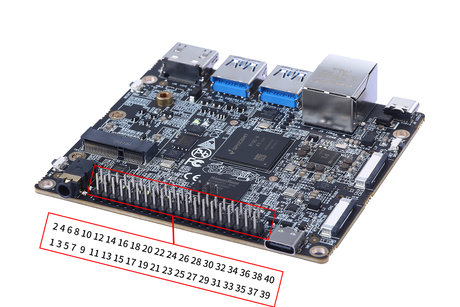
K1 reserves a 40-pin GPIO extension interface, using a 2.54 double-row straight insertion socket, which is convenient for enthusiasts to connect peripherals according to their own needs and expand different functions. Our system will set these IOs to some specific functions by default, but users can reconfigure them through software to make these general-purpose IOs have some special functions, because these IOs are all multi-functional multiplexed pins.

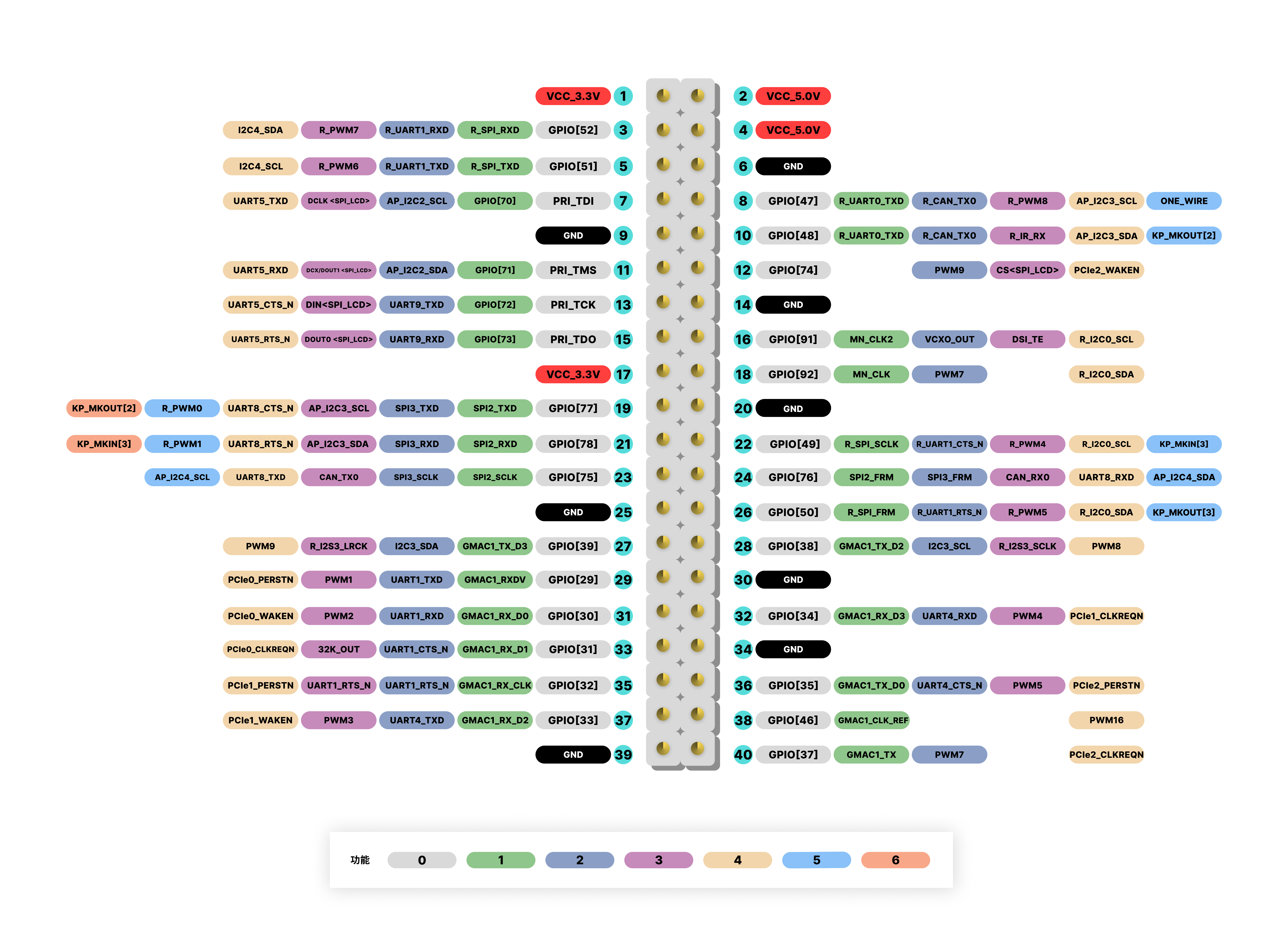
1. Pin Definition

2. Multifunctional Pin Definition List
All GPIOs can be set as general-purpose inputs or outputs, and can also be configured into more functions through the kernel. The following table shows the extended functions of each GPIO.
https://developer.spacemit.com/documentation?token=An1vwTwKaigaXRkYfwmcznTXned
| Pin Number | Function 0 | Function 1 | Function 2 | Function 3 | Function 4 | Function 5 | Function 6 | Function 7 |
|---|---|---|---|---|---|---|---|---|
| 3 | GPIO[52] | R_SPI_RXD | R_UART1_RXD | R_PWM7 | I2C4_SDA | |||
| 5 | GPIO[51] | R_SPI_TXD | R_UART1_TXD | R_PWM6 | I2C4_SCL | |||
| 7 | PRI_TDI | GPIO[70] | AP_I2C2_SCL | DCLK <SPI_LCD> | UART5_TXD | |||
| 8 | GPIO[47] | R_UART0_TXD | R_CAN_TX0 | R_PWM8 | AP_I2C3_SCL | ONE_WIRE | ||
| 10 | GPIO[48] | R_UART0_RXD | R_CAN_RX0 | R_IR_RX | AP_I2C3_SDA | KP_MKOUT[2] | ||
| 11 | PRI_TMS | GPIO[71] | AP_I2C2_SDA | DCX/DOUT1 <SPI_LCD> | UART5_RXD | |||
| 12 | GPIO[74] | PWM9 | CS<SPI_LCD> | PCIe2_WAKEN | ||||
| 13 | PRI_TCK | GPIO[72] | UART9_TXD | DIN<SPI_LCD> | UART5_CTS_N | |||
| 15 | PRI_TDO | GPIO[73] | UART9_RXD | DOUT0 <SPI_LCD> | UART5_RTS_N | |||
| 16 | GPIO[91] | MN_CLK2 | VCXO_OUT | DSI_TE | R_I2C0_SCL | |||
| 18 | GPIO[92] | MN_CLK | PWM7 | R_I2C0_SDA | ||||
| 19 | GPIO[77] | SPI2_TXD | SPI3_TXD | AP_I2C3_SCL | UART8_CTS_N | R_PWM0 | KP_MKOUT[2] | |
| 20 | GPIO[49] | R_SPI_SCLK | R_UART1_CTS_N | R_PWM4 | R_I2C0_SCL | KP_MKIN[3] | ||
| 21 | GPIO[78] | SPI2_RXD | SPI3_RXD | AP_I2C3_SDA | UART8_RTS_N | R_PWM1 | KP_MKIN[3] | |
| 23 | GPIO[75] | SPI2_SCLK | SPI3_SCLK | CAN_TX0 | UART8_TXD | AP_I2C4_SCL | ||
| 24 | GPIO[76] | SPI2_FRM | SPI3_FRM | CAN_RX0 | UART8_RXD | AP_I2C4_SDA | ||
| 26 | GPIO[50] | R_SPI_FRM | R_UART1_RTS_N | R_PWM5 | R_I2C0_SDA | KP_MKOUT[3] | ||
| 27 | GPIO[39] | GMAC1_TX_D3 | I2C3_SDA | R_I2S3_LRCK | PWM9 | |||
| 28 | GPIO[38] | GMAC1_TX_D2 | I2C3_SCL | R_I2S3_SCLK | PWM8 | |||
| 29 | GPIO[29] | GMAC1_RXDV | UART1_TXD | PWM1 | PCIe0_PERSTN | |||
| 31 | GPIO[30] | GMAC1_RX_D0 | UART1_RXD | PWM2 | PCIe0_WAKEN | |||
| 32 | GPIO[34] | GMAC1_RX_D3 | UART4_RXD | PWM4 | PCIe1_CLKREQN | |||
| 33 | GPIO[31] | GMAC1_RX_D1 | UART1_CTS_N | 32K_OUT | PCIe0_CLKREQN | |||
| 35 | GPIO[32] | GMAC1_RX_CLK | UART1_RTS_N | MN_CLK | PCIe1_PERSTN | |||
| 36 | GPIO[35] | GMAC1_TX_D0 | UART4_CTS_N | PWM5 | PCIe2_PERSTN | |||
| 37 | GPIO[33] | GMAC1_RX_D2 | UART4_TXD | PWM3 | PCIe1_WAKEN | |||
| 38 | GPIO[46] | GMAC1_CLK_REF | PWM16 | |||||
| 40 | GPIO[37] | GMAC1_TX | PWM7 | PCIe2_CLKREQN |
Remarks:
Voltage
All 3.3V, 5V, and ground on the board are not configurable, and all remaining pins are 3.3V, that is, the input and output of the GPIO are 3.3V. Of course, these pins are not 3.3V from the chip end, but all IOs are converted to 3.3V through level conversion.
Input and Output
The high level of the GPIO is set to 3.3V, and the low level is 0V.

